- 您现在的位置:买卖IC网 > PDF目录30737 > LC89051V SPECIALTY CONSUMER CIRCUIT, PDSO24 PDF资料下载
参数资料
| 型号: | LC89051V |
| 元件分类: | 消费家电 |
| 英文描述: | SPECIALTY CONSUMER CIRCUIT, PDSO24 |
| 封装: | SSOP-24 |
| 文件页数: | 14/15页 |
| 文件大小: | 274K |
| 代理商: | LC89051V |
Functions
1. Data Input and Output (DIN1, DIN2, E/DOUT)
The DIN1 pin has a built-in amplifier, and can receive signals with an amplitude of about 400 mVp-p (coaxial input).
The DIN2 pin is only for use in optical modules.
Note that although the data input pins are controlled by the microcontroller, DIN1 can be selected when a
microcontroller is not used. The microcontroller interface pins must be tied low in such applications.
The E/DOUT normally outputs channel status information. However, it can be set to output either the input bi-phase
data or the validity flag by command codes from the microcontroller.
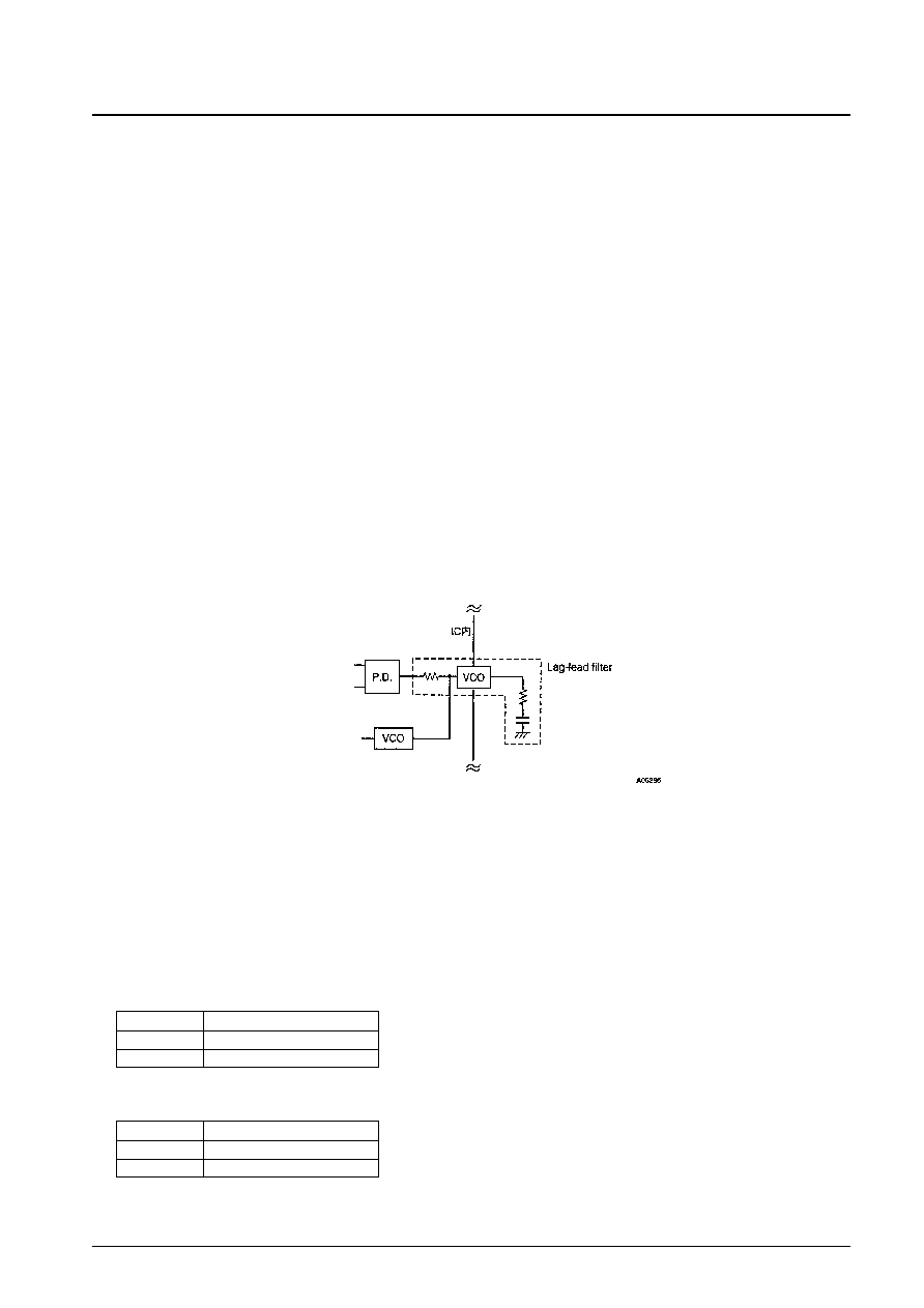
2. PLL (R, VIN, VCO, AVOCK)
This circuit includes a built-in VCO and supports sampling frequencies of 32, 44.1, and 48 kHz.
This LSI can also receive at the 2
× sampling frequencies of 64 kHz, 88.2 kHz, and 96 kHz, but only when operating
from a 5-V power-supply voltage. However, the demodulated data and clock output during double speed reception
follow the received sampling frequency, and the transmission format for 2
×-speed data must follow the IEC958
standard.
The built-in VCO is controlled by the resistors connected to the R and VIN pins.
The resistor connected to R functions as both the VCO gain control and as temperature compensation. The VIN pin
sets the VCO free-running frequency. Recommended circuit constants are shown in the sample application circuit.
Note that the VCO free-running frequency varies with temperature and with manufacturing variations between
samples. The recommended circuit constants shown in the sample application circuit take these variations into
account so that the PLL circuit lockup characteristics are not adversely affected. These values are not designed to
reduce variations in the free-running frequency. The VCO pin is the PLL loop filter pin. The loop filter is formed by
attaching an external capacitor and a resistor to this pin. See the sample application circuit for these circuit constants.
PLL Loop Filter Structure
The PLL circuit will be reset within a fixed period when PLL lock pull-in fails if a continuously operating clock of
no more than 50 kHz is input to the AVOCK pin. This allows incorrect PLL operation to be avoided.
3. Clock Settings and Output (FS128, BCK, LRCK, DATAOUT, CKSEL, CKOUT)
A 128fs clock signal is output from the FS128 pin. Figure 1 shows the output timing for the BCK, LRCK, and
DATAOUT pins.
The CKOUT clock output is set by the CKSEL pin as listed in the table below.
The microcontroller interface format is also set by CKSEL as listed in the table below.
No. 5543-8/15
LC89051V
CKSEL
CKOUT
L
384fs clock output
H
512fs clock output
CKSEL
Microcontroller interface
L
Figure 2
H
Figure 3
相关PDF资料 |
PDF描述 |
|---|---|
| LC89052TA-E | SPECIALTY CONSUMER CIRCUIT, PDSO24 |
| LC890561W | SPECIALTY CONSUMER CIRCUIT, PQFP48 |
| LC890561W | SPECIALTY CONSUMER CIRCUIT, PQFP48 |
| LC89057W-VF4-E | SPECIALTY CONSUMER CIRCUIT, PQFP48 |
| LC89057W-VF4A-E | SPECIALTY CONSUMER CIRCUIT, PQFP48 |
相关代理商/技术参数 |
参数描述 |
|---|---|
| LC89052T | 制造商:SANYO 制造商全称:Sanyo Semicon Device 功能描述:Digital Audio Interface Receiver |
| LC89052TA-E | 功能描述:音频发送器、接收器、收发器 RoHS:否 制造商:Cirrus Logic 工作电源电压:3.3 V, 5 V 电源电流:11.8 mA 通道数量:1 最大工作温度:+ 70 C 接口类型:I2C, SPI 安装风格:SMD/SMT 封装 / 箱体:TSSOP-28 封装: |
| LC89052TA-TLM-E | 功能描述:音频发送器、接收器、收发器 RoHS:否 制造商:Cirrus Logic 工作电源电压:3.3 V, 5 V 电源电流:11.8 mA 通道数量:1 最大工作温度:+ 70 C 接口类型:I2C, SPI 安装风格:SMD/SMT 封装 / 箱体:TSSOP-28 封装: |
| LC89052THS-E | 制造商:ON Semiconductor 功能描述:AUDIO I/F RECEIVER |
| LC890561W | 制造商:SANYO 制造商全称:Sanyo Semicon Device 功能描述:CMOS IC Digital Audio Interface Receiver with Built-in Data Buffer Memory |
发布紧急采购,3分钟左右您将得到回复。