- 您现在的位置:买卖IC网 > PDF目录30737 > LC89052TA-E SPECIALTY CONSUMER CIRCUIT, PDSO24 PDF资料下载
参数资料
| 型号: | LC89052TA-E |
| 元件分类: | 消费家电 |
| 英文描述: | SPECIALTY CONSUMER CIRCUIT, PDSO24 |
| 封装: | 0.225 INCH, TSSOP-24 |
| 文件页数: | 4/42页 |
| 文件大小: | 224K |
| 代理商: | LC89052TA-E |
第1页第2页第3页当前第4页第5页第6页第7页第8页第9页第10页第11页第12页第13页第14页第15页第16页第17页第18页第19页第20页第21页第22页第23页第24页第25页第26页第27页第28页第29页第30页第31页第32页第33页第34页第35页第36页第37页第38页第39页第40页第41页第42页
LC89052TA-E
No.7457-12/42
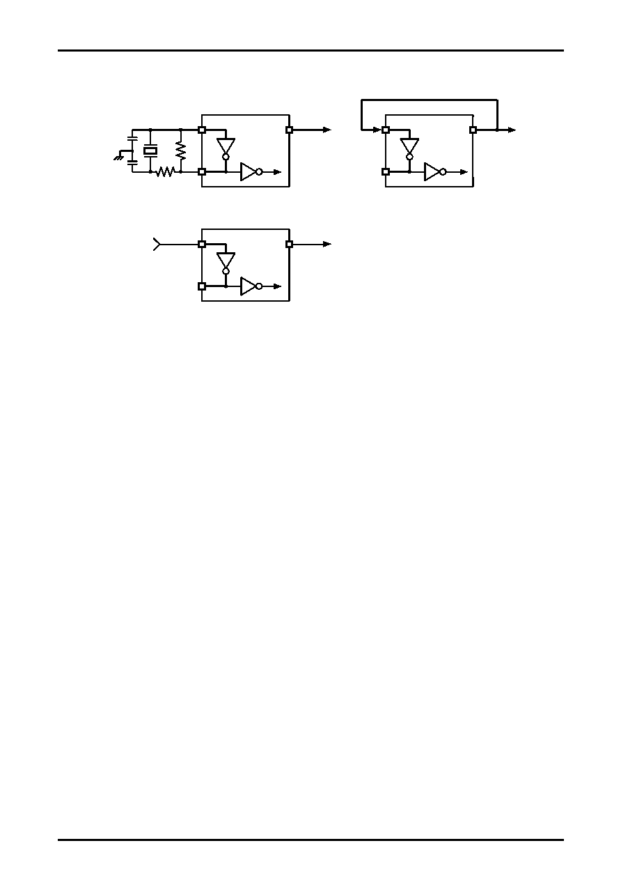
8.3.2 Oscillator amplifier (XIN and XOUT)
The following methods can be used to supply the clock signal to the internal oscillator amplifier.
Figure 8.3 XIN and XOUT Pin Circuit Configurations
When you connect an oscillator, use the one with the fundamental frequency. Since the load capacitance depends on
the oscillator characteristics, give careful consideration.
Since the clock supplied to the XIN pin is normally used for the following purposes, the clock signal should be
present all the time.
—Externally supplied clock used when the PLL circuit is unlocked and when XIN is the clock source
—For calculation of sampling frequencies of the input data
Input a clock with a frequency of 11.2896M, 12.288M, 16.9344M, 22.5792M, 24.576M, or 33.8688MHz according to
the setting of the XISEL[2:0]. Input digital data only after the XISEL[2:0] has been set to match the set frequency and
the oscillator or external clock input frequency. The LC89052TA-E may malfunction if data is input when the input
frequency and the set frequency are not consistent.
The LC89052TA-E operates even when the frequency set with the XISEL[2:0] and the frequency supplied to the XIN
pin are different. However, continuity at clock switching time and correct input fs calculation are not guaranteed.
The LC89052TA-E supports a structure in which CKOUT pin is connected to the XIN pin to set XISEL3, requiring
no oscillator. However, since only VCO can be used as the source clock, the VCO free-running frequency (10M to
16MHz) is output from the CKOUT pin when the PLL is not locked. Furthermore, input fs calculation and limitation
are impossible with this approach. Also, since no clock is supplied to the oscillator amplifier circuit when the VCO is
set to stop, the whole system stops. This function is available only for the PLLCK[1:0] = "00" setting, which is 256fs.
Other system clock settings might cause malfunction.
Normally the oscillator amplifier stops automatically when the PLL is locked. It is possible to change to a continuous
operation mode with AMPCNT. Setting the LC89052TA-E to the continuous operation mode makes it possible to
calculate the input sampling frequency even when the PLL is locked. However, since both the oscillator amplifier
clock and the PLL clock signals coexist in that case the user must pay attention and make sure audio quality is not
adversely affected.
The oscillator amplifier can be stopped when not required by setting the AMPOPR. However, the application must
maintain its state for at least 10ms until the oscillator stabilizes, when returning from stop to operation mode. After
that the LC89052TA-E must be returned to the normal operation mode.
XIN
XOUT
CKOUT
XIN
XOUT
CKOUT
XIN
XOUT
CKOUT
(a) Oscillator element
(c) CKOUT clock signal
(b) External clock signal
相关PDF资料 |
PDF描述 |
|---|---|
| LC890561W | SPECIALTY CONSUMER CIRCUIT, PQFP48 |
| LC890561W | SPECIALTY CONSUMER CIRCUIT, PQFP48 |
| LC89057W-VF4-E | SPECIALTY CONSUMER CIRCUIT, PQFP48 |
| LC89057W-VF4A-E | SPECIALTY CONSUMER CIRCUIT, PQFP48 |
| LC89057W-VF4 | SPECIALTY CONSUMER CIRCUIT, PQFP48 |
相关代理商/技术参数 |
参数描述 |
|---|---|
| LC89052TA-TLM-E | 功能描述:音频发送器、接收器、收发器 RoHS:否 制造商:Cirrus Logic 工作电源电压:3.3 V, 5 V 电源电流:11.8 mA 通道数量:1 最大工作温度:+ 70 C 接口类型:I2C, SPI 安装风格:SMD/SMT 封装 / 箱体:TSSOP-28 封装: |
| LC89052THS-E | 制造商:ON Semiconductor 功能描述:AUDIO I/F RECEIVER |
| LC890561W | 制造商:SANYO 制造商全称:Sanyo Semicon Device 功能描述:CMOS IC Digital Audio Interface Receiver with Built-in Data Buffer Memory |
| LC890561W-E | 功能描述:音频发送器、接收器、收发器 RoHS:否 制造商:Cirrus Logic 工作电源电压:3.3 V, 5 V 电源电流:11.8 mA 通道数量:1 最大工作温度:+ 70 C 接口类型:I2C, SPI 安装风格:SMD/SMT 封装 / 箱体:TSSOP-28 封装: |
| LC89056W-E | 功能描述:音频发送器、接收器、收发器 RoHS:否 制造商:Cirrus Logic 工作电源电压:3.3 V, 5 V 电源电流:11.8 mA 通道数量:1 最大工作温度:+ 70 C 接口类型:I2C, SPI 安装风格:SMD/SMT 封装 / 箱体:TSSOP-28 封装: |
发布紧急采购,3分钟左右您将得到回复。