- 您现在的位置:买卖IC网 > PDF目录39192 > LC89080 TRIPLE, PARALLEL, 8 BITS INPUT LOADING, 8-BIT DAC, PDIP42 PDF资料下载
参数资料
| 型号: | LC89080 |
| 元件分类: | DAC |
| 英文描述: | TRIPLE, PARALLEL, 8 BITS INPUT LOADING, 8-BIT DAC, PDIP42 |
| 封装: | SDIP-42 |
| 文件页数: | 3/8页 |
| 文件大小: | 106K |
| 代理商: | LC89080 |
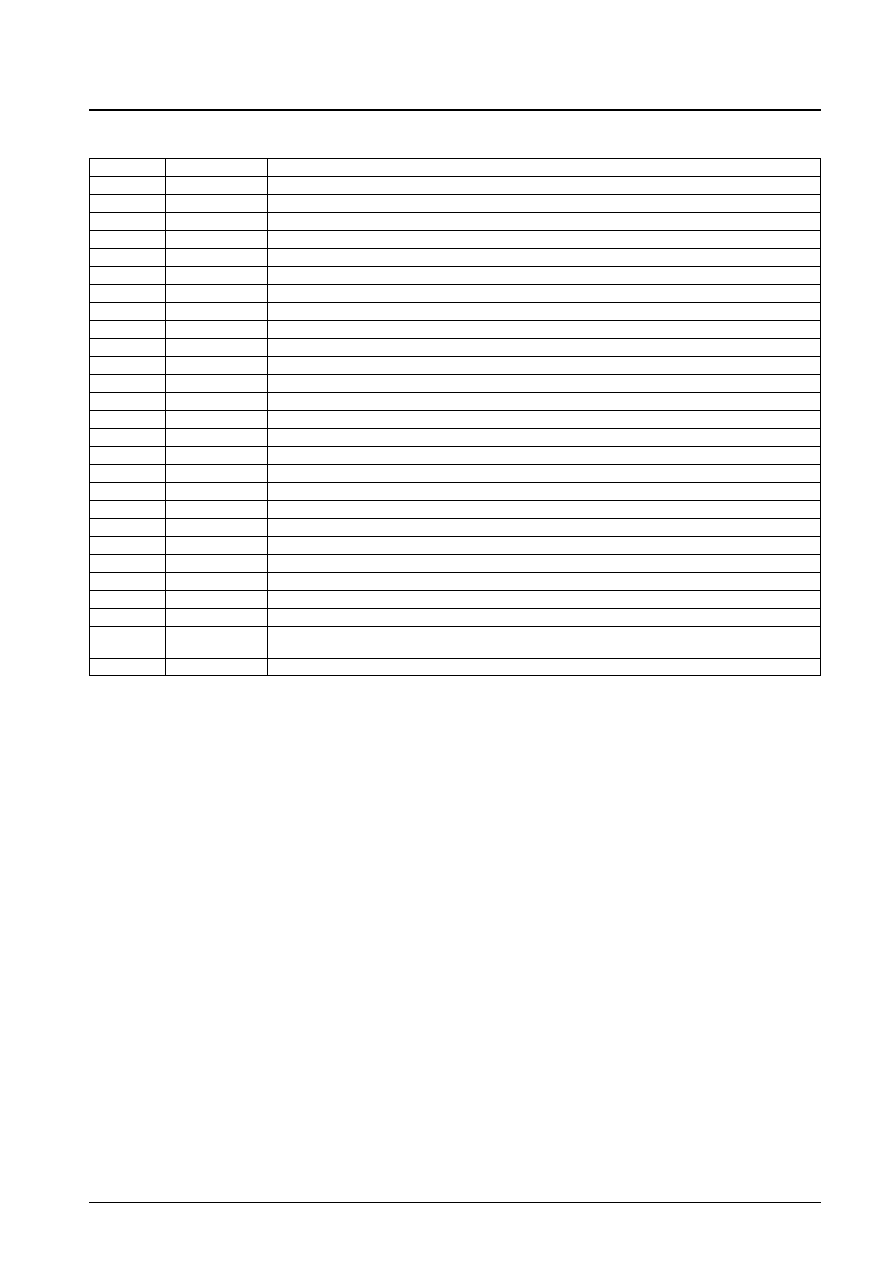
Pin Assignment LC89080 (DIP42S)
No. 4030-3/8
LC89080, 89080Q
Pin No.
Symbol
Description
1
DVDD
Digital system power supply (+5 V)
2
DA1
Channel A digital input (MSB)
3 to 8
DA2 to DA7
Channel A digital input
9
DA8
Channel A digital input (LSB)
10
DB1
Channel B digital input (MSB)
11 to 16
DB2 to DB7
Channel B digital input
17
DB8
Channel B digital input (LSB)
18
DC1
Channel C digital input (MSB)
19 to 24
DC2 to DC7
Channel C digital input
25
DC8
Channel C digital input (LSB)
26
CLK
Clock input
27
DVDD
Digital system power supply (+5 V)
28
DGND
Digital system ground (0 V)
29
ICOB
Channel C negative output. Connect to A.GND through an output resistor RO (usually 75 ).
30
ICO
Channel C positive output. Connect to A.GND through an output resistor RO (usually 75 ).
31
AVDD
Analog system power supply (+5 V)
32
IBOB
Channel B negative output. Connect to A.GND through an output resistor RO (usually 75 ).
33
IBO
Channel B positive output. Connect to A.GND through an output resistor RO (usually 75 ).
34
AGND
Analog system ground (0 V)
35
IAOB
Channel A negative output. Connect to A.GND through an output resistor RO (usually 75 ).
36
IAO
Channel A positive output. Connect to A.GND through an output resistor RO (usually 75 ).
37
AVDD
Analog system power supply (+5 V)
38
COMP
Phase compensation capacitor. Connect a 1 F capacitor between this pin and ground.
39
IREF
Reference current output. Connect a resistor that is 4 times the output resistance RO to this pin.
40
VREFIN
Reference voltage input. This input pin sets the analog output dynamic range.
41
VREFOUT
Reference voltage output. The output voltage is set to 0.2 times VDD by a resistor divider.
When VDD is 5.0 V, a 1.0 V reference voltage can be acquired from pin 40.
42
DGND
Digital system ground (0 V)
相关PDF资料 |
PDF描述 |
|---|---|
| LC89080Q | TRIPLE, PARALLEL, 8 BITS INPUT LOADING, 8-BIT DAC, PQFP48 |
| LC89081Q | PARALLEL, 8 BITS INPUT LOADING, 8-BIT DAC, PQFP44 |
| LC89086M | 1-CH 8-BIT PROPRIETARY METHOD ADC, PARALLEL ACCESS, PDSO24 |
| LC89170M | SPECIALTY CONSUMER CIRCUIT, PDSO14 |
| LC8992 | SPECIALTY CONSUMER CIRCUIT, PDIP8 |
相关代理商/技术参数 |
参数描述 |
|---|---|
| LC89080Q | 制造商:SANYO 制造商全称:Sanyo Semicon Device 功能描述:Video Signal 3-Channel 8-Bit D/A Converter |
| LC89081Q | 制造商:未知厂家 制造商全称:未知厂家 功能描述: |
| LC89086 | 制造商:未知厂家 制造商全称:未知厂家 功能描述:Analog-to-Digital Converter, 8-Bit |
| LC89086M | 制造商:SANYO 制造商全称:Sanyo Semicon Device 功能描述:8 Bit A/D Converter |
| LC89091JAGEVK | 制造商:ON Semiconductor 功能描述:EVAL BD FOR LC89091JA - Bulk 制造商:ON Semiconductor 功能描述:KIT EVAL FOR LC89091JA |
发布紧急采购,3分钟左右您将得到回复。