- 您现在的位置:买卖IC网 > PDF目录67755 > LC99403 SPECIALTY ANALOG CIRCUIT, BGA180 PDF资料下载
参数资料
| 型号: | LC99403 |
| 元件分类: | 模拟信号调理 |
| 英文描述: | SPECIALTY ANALOG CIRCUIT, BGA180 |
| 封装: | 7.50 X 7.50 MM, ISB-180 |
| 文件页数: | 9/12页 |
| 文件大小: | 116K |
| 代理商: | LC99403 |
LC99403
No.A1065-6/12
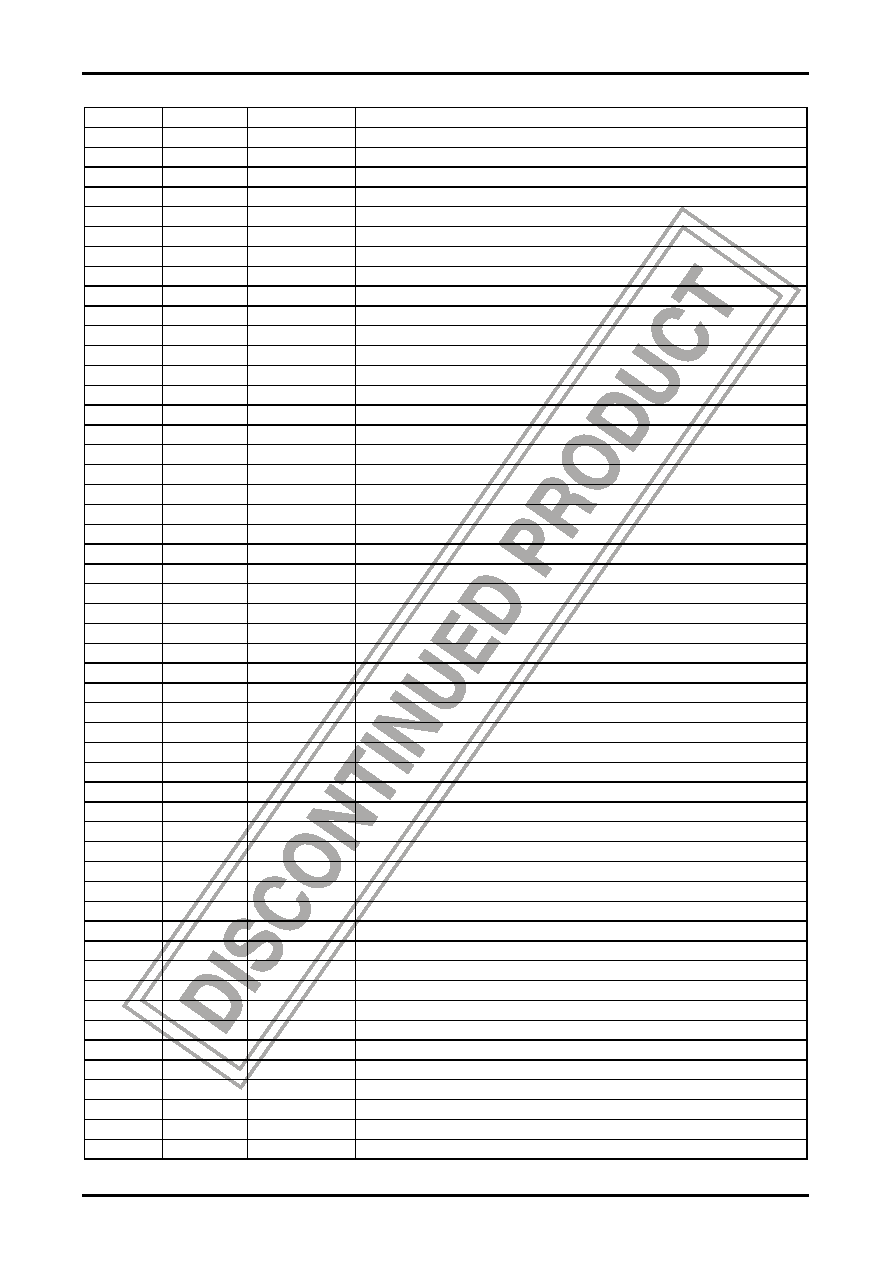
Detailed Pin Descriptions
Ball No.
Type
Pin name
Description
A1
-
NC
A2
-
NC
A3
DRO
HTR
Output block reset pulse for CCD
A4
DRO
HT1
CCD horizontal transfer pulse output
A5
DO2
IO3
Unused. (The pin must be OPEN.)
A6
DO2
IO7
Unused. (The pin must be OPEN.)
A7
DO2
IO11
EXPIN_OUT2 (The setting of Register Address A_0x2C is output.)
A8
DO2
IO13
EXPIN_OUT4 (The setting of Register Address A_0x2C is output.)
A9
DO2
IO16
Unused. (The pin must be OPEN.)
A10
-
NC
A11
DO2
IO22
Unused. (The pin must be OPEN.)
A12
DO2
IO26
Unused. (The pin must be OPEN.)
A13
DI2
IO28
Unused. (The pin must be fixed to GND.)
A14
-
NC
B1
DO1
CCD
Output for CCD_VDD
B2
VSS
VSS (REG)
GND of regulator
B3
VSS
GND of digital system
B4
DI2
IO1
STB (When stand-by, this pin is involved in the settings of I/O condition.)
B5
DO2
IO4
Unused. (The pin must be OPEN.)
B6
DO2
IO5
Unused. (The pin must be OPEN.)
B7
DO2
IO9
EXPIN_OUT0 (The setting of Register Address A_0x2C is output.)
B8
DO2
IO14
EXPIN_OUT5 (The setting of Register Address A_0x2C is output.)
B9
VDD2
VDD(I/O)
VDD of I/O system
B10
DO2
IO18
Unused. (The pin must be OPEN.)
B11
DO2
IO24
Unused. (The pin must be OPEN.)
B12
-
NC
B13
VSS
GND of digital system
B14
DO2
PCLK
Synchronized clock output of digital data
C1
AO
CAP0
AFE test pin
C2
VDD3
VDD (LOG)
Internal logic VDD
C3
AO
REFH
ADC reference voltage follower output at high
C4
DIO2
IO0
VRES (External V-synchronized reset signal can be input. Low: Reset)
C5
-
NC
C6
DO2
IO6
Unused. (The pin must be OPEN.)
C7
DO2
IO8
Unused. (The pin must be OPEN.)
C8
DO2
IO15
EXPIN_OUT6 (The setting of Register Address A_0x2C is output.)
C9
DO2
IV20
Unused. (The pin must be OPEN.)
C10
DO2
IO23
Unused. (The pin must be OPEN.)
C11
VSS
GND of digital system
C12
VDD3
VDD (LOG)
Internal logic VDD
C13
VSS
GND of digital system
C14
VDD2
VDD (I/O)
VDD of I/O system
D1
AI
CINB
AFE test pin
D2
AI
CINS
Image signal input pin from CCD
D3
-
NC
D4
DRO
HT2
CCD horizontal transfer pulse output
D5
DO2
IO10
EXPIN_OUT1 (The setting of Register Address A_0x2C is output.)
D6
VSS
GND for digital system
D7
DO2
IO12
EXPIN_OUT3 (The setting of Register Address A_0x2C is output.)
D8
DO2
IO17
Unused. (The pin must be OPEN.)
D9
DO2
IO21
Unused. (The pin must be OPEN.)
D10
DO2
IO25
Unused. (The pin must be OPEN.)
Continued on next page.
相关PDF资料 |
PDF描述 |
|---|---|
| LGDS-300-0-K/S | 1-OUTPUT DC-DC REG PWR SUPPLY MODULE |
| LGDS-300-0-K/T | 1-OUTPUT DC-DC REG PWR SUPPLY MODULE |
| LM10506TMX | 1-CHANNEL POWER SUPPLY SUPPORT CKT, PBGA34 |
| LM10506TME | 1-CHANNEL POWER SUPPLY SUPPORT CKT, PBGA34 |
| LM10506TMX-A | 1-CHANNEL POWER SUPPLY SUPPORT CKT, PBGA34 |
相关代理商/技术参数 |
参数描述 |
|---|---|
| LC9943 | 制造商:未知厂家 制造商全称:未知厂家 功能描述:Optoelectronic |
| LC9945 | 制造商:SANYO 制造商全称:Sanyo Semicon Device 功能描述:1/6 Inch Optical Size CCIR Black-and-White Solid-State Imaging Device |
| LC99452 | 制造商:未知厂家 制造商全称:未知厂家 功能描述: |
| LC9946 | 制造商:SANYO 制造商全称:Sanyo Semicon Device 功能描述:1/6 Inch Optical Size EIA Black-and-White Solid-State Imaging Device |
| LC9947G | 制造商:SANYO 制造商全称:Sanyo Semicon Device 功能描述:1/5 Inch Optical Size EIA Black-and-White Solid-State Imaging Device |
发布紧急采购,3分钟左右您将得到回复。