- 您现在的位置:买卖IC网 > PDF目录43903 > LC9997M SPECIALTY ANALOG CIRCUIT, DFM20 PDF资料下载
参数资料
| 型号: | LC9997M |
| 元件分类: | 模拟信号调理 |
| 英文描述: | SPECIALTY ANALOG CIRCUIT, DFM20 |
| 封装: | DIP-20 |
| 文件页数: | 8/11页 |
| 文件大小: | 212K |
| 代理商: | LC9997M |
Notes: 3. This voltage must not exceed the substrate pulse low level VLSUB.
4. These input pins are high-impedance inputs.
No. 5783-6/11
LC9997M
Parameter
Symbol
Conditions
Ratings
Unit
min
typ
max
DC operating current
IDD
4.5
7.0
11.0
mA
DC Characteristics
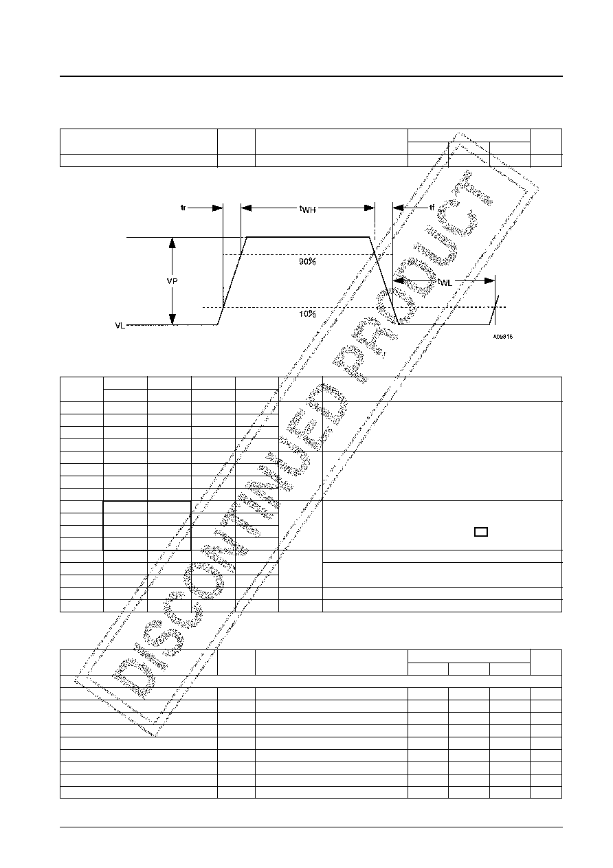
Drive Pulse Waveform Stipulations
Pulse Waveform Figure
Symbol
tWH
tWL
tr
tf
Unit
Notes
typ
φ 1
166
100
6.5
φ 2
141
116
11
ns
Frame transfer time
φ 3
166
100
6.5
When the frame shift frequency is 3.58 MHz
φ 4
141
116
11
φ S1
141
116
11
φ S2
141
116
11
ns
Frame transfer time
φ S3
141
116
11
When the frame shift frequency is 3.58 MHz
φ S4
141
116
11
φ S1
1.36
62.1
30
φ S2
1.36
62.1
30
ns
Vertical transfer time for a single horizontal line
φ S3
62.1
1.36
30
Values in the box enclosed in the darker lines
are in microseconds.
φ S4
62.1
1.36
30
φ R
11
86
4
Reset pulse
φ H1
50
49
3
ns
Horizontal transfer time
φ H2
50
49
3
φ NSUB
9.9
16.59*
0.07
1
s
Slice pulse
φ NSUB
4.2
16.59*
0.07
1
s
Shutter pulse
Parameter
Symbol
Conditions
Ratings
Unit
min
typ
max
[Sensitivity]
Luminance signal
S
Test method 1
130
mV
R gain
GR
Test method 1
0.7
2.4
B gain
GB
Test method 1
2.0
4.4
Image signal uninformity
VF
Test method 2
15
%
Saturation signal
Vsat
Test method 3, *5
600
mV
Smear
SM
Test method 4, *6
0.04
%
Dark signal
Vdrk
Test method 5. Ta = 55°C7
mV
Color irregularity (mura)
Vcs
Test method 6
50
mV
Gamma characteristics
γ
1
Imaging Characteristics (storage time = 1/60 s) at Ta = 25°C
Notes: 5. When the substrate pulse VHSUB is used fixed at 40±2 V, the minimum saturation output is 450 mV.
6. When the frame shift frequency is 3.58 MHz and the storage time is 1/60 s.
Note: The item marked with an asterisk (*) is in milliseconds.
VP: Pulse amplitude
VL: Low level
相关PDF资料 |
PDF描述 |
|---|---|
| LDO10C-005W05-VXJ | DC-DC REG PWR SUPPLY MODULE |
| LDO10C-005W05-SXJ | DC-DC REG PWR SUPPLY MODULE |
| LEN-1.8/28-D12MH | 1-OUTPUT 0.25 W DC-DC REG PWR SUPPLY MODULE |
| LEN-1.8/28-D12MH | 1-OUTPUT 0.25 W DC-DC REG PWR SUPPLY MODULE |
| LEN-1.8/28-D12M | 1-OUTPUT 0.25 W DC-DC REG PWR SUPPLY MODULE |
相关代理商/技术参数 |
参数描述 |
|---|---|
| LC9998G | 制造商:SANYO 制造商全称:Sanyo Semicon Device 功能描述:1/5 Optical Size PAL Color Solid-State Image Sensor |
| LCA | 制造商:CK-COMPONENTS 制造商全称:C&K Components 功能描述:Subminiature Snap-acting Switches |
| LCA0011210 | 制造商:Carlo Gavazzi 功能描述:LCA0011210 |
| LCA0011216 | 制造商:Carlo Gavazzi 功能描述:LCA0011216 |
| LCA0014816 | 制造商:Carlo Gavazzi 功能描述:LCA0014816 |
发布紧急采购,3分钟左右您将得到回复。