- 您现在的位置:买卖IC网 > PDF目录177784 > LCMXO1200C-5FT256C (LATTICE SEMICONDUCTOR CORP) PDF资料下载
参数资料
| 型号: | LCMXO1200C-5FT256C |
| 厂商: | LATTICE SEMICONDUCTOR CORP |
| 元件分类: | PLD |
| 中文描述: | FLASH PLD, 3.6 ns, PBGA256 |
| 封装: | 17 X 17 MM, FTBGA-256 |
| 文件页数: | 78/96页 |
| 文件大小: | 1389K |
| 代理商: | LCMXO1200C-5FT256C |
第1页第2页第3页第4页第5页第6页第7页第8页第9页第10页第11页第12页第13页第14页第15页第16页第17页第18页第19页第20页第21页第22页第23页第24页第25页第26页第27页第28页第29页第30页第31页第32页第33页第34页第35页第36页第37页第38页第39页第40页第41页第42页第43页第44页第45页第46页第47页第48页第49页第50页第51页第52页第53页第54页第55页第56页第57页第58页第59页第60页第61页第62页第63页第64页第65页第66页第67页第68页第69页第70页第71页第72页第73页第74页第75页第76页第77页当前第78页第79页第80页第81页第82页第83页第84页第85页第86页第87页第88页第89页第90页第91页第92页第93页第94页第95页第96页
2-5
Architecture
Lattice Semiconductor
MachXO Family Data Sheet
Modes of Operation
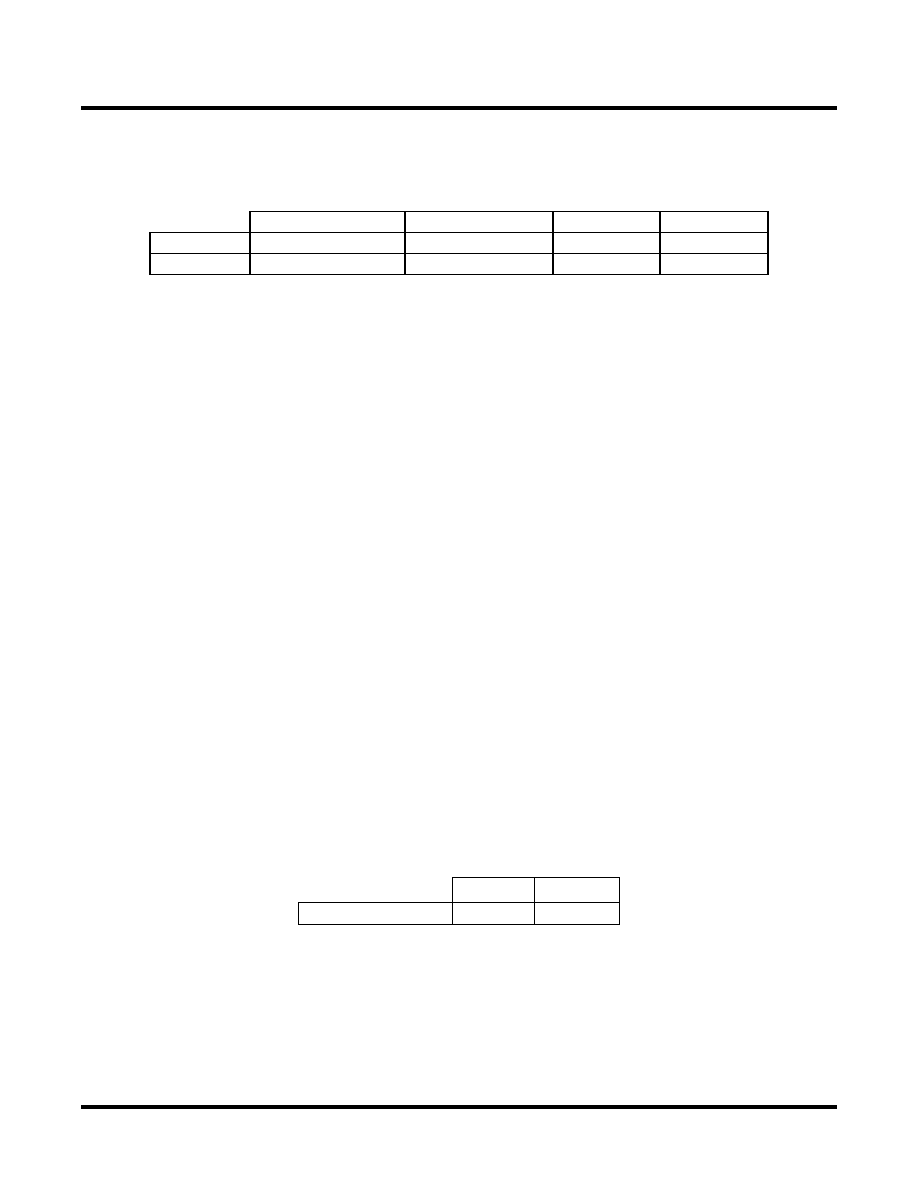
Each Slice is capable of four modes of operation: Logic, Ripple, RAM, and ROM. The Slice in the PFF is capable of
all modes except RAM. Table 2-2 lists the modes and the capability of the Slice blocks.
Table 2-2. Slice Modes
Logic Mode: In this mode, the LUTs in each Slice are configured as 4-input combinatorial lookup tables (LUT4). A
LUT4 can have 16 possible input combinations. Any logic function with four inputs can be generated by program-
ming this lookup table. Since there are two LUT4s per Slice, a LUT5 can be constructed within one Slice. Larger
lookup tables such as LUT6, LUT7, and LUT8 can be constructed by concatenating other Slices.
Ripple Mode: Ripple mode allows the efficient implementation of small arithmetic functions. In ripple mode, the fol-
lowing functions can be implemented by each Slice:
Addition 2-bit
Subtraction 2-bit
Add/Subtract 2-bit using dynamic control
Up counter 2-bit
Down counter 2-bit
Ripple mode multiplier building block
Comparator functions of A and B inputs
- A greater-than-or-equal-to B
- A not-equal-to B
- A less-than-or-equal-to B
Two additional signals, Carry Generate and Carry Propagate, are generated per Slice in this mode, allowing fast
arithmetic functions to be constructed by concatenating Slices.
RAM Mode: In this mode, distributed RAM can be constructed using each LUT block as a 16x2-bit memory.
Through the combination of LUTs and Slices, a variety of different memories can be constructed.
The ispLEVER design tool supports the creation of a variety of different size memories. Where appropriate, the
software will construct these using distributed memory primitives that represent the capabilities of the PFU.
Table 2-3 shows the number of Slices required to implement different distributed RAM primitives. Figure 2-6 shows
the distributed memory primitive block diagrams. Dual port memories involve the pairing of two Slices. One Slice
functions as the read-write port, while the other companion Slice supports the read-only port. For more information
on RAM mode in MachXO devices, please see details of additional technical documentation at the end of this data
sheet.
Table 2-3. Number of Slices Required For Implementing Distributed RAM
Logic
Ripple
RAM
ROM
PFU Slice
LUT 4x2 or LUT 5x1
2-bit Arithmetic Unit
SP 16x2
ROM 16x1 x 2
PFF Slice
LUT 4x2 or LUT 5x1
2-bit Arithmetic Unit
N/A
ROM 16x1 x 2
SPR16x2
DPR16x2
Number of Slices
1
2
Note: SPR = Single Port RAM, DPR = Dual Port RAM
相关PDF资料 |
PDF描述 |
|---|---|
| LCMXO1200C-3T100I | |
| LCMXO1200E-4FT256I | |
| LCMXO640C-4M100C | |
| LCMXO640E-5B256C | |
| LCMXO2280E-3B256I | |
相关代理商/技术参数 |
参数描述 |
|---|---|
| LCMXO1200C-5FTN256C | 功能描述:CPLD - 复杂可编程逻辑器件 1200 LUTS 211 I/O RoHS:否 制造商:Lattice 系列: 存储类型:EEPROM 大电池数量:128 最大工作频率:333 MHz 延迟时间:2.7 ns 可编程输入/输出端数量:64 工作电源电压:3.3 V 最大工作温度:+ 90 C 最小工作温度:0 C 封装 / 箱体:TQFP-100 |
| LCMXO1200C-5M132C | 功能描述:CPLD - 复杂可编程逻辑器件 1200 LUTs 101 IO 1.8 /2.5/3.3V -5 Spd RoHS:否 制造商:Lattice 系列: 存储类型:EEPROM 大电池数量:128 最大工作频率:333 MHz 延迟时间:2.7 ns 可编程输入/输出端数量:64 工作电源电压:3.3 V 最大工作温度:+ 90 C 最小工作温度:0 C 封装 / 箱体:TQFP-100 |
| LCMXO1200C-5MN132C | 功能描述:CPLD - 复杂可编程逻辑器件 1200 LUTs 101 IO 1.8 /2.5/3.3V -5 Spd RoHS:否 制造商:Lattice 系列: 存储类型:EEPROM 大电池数量:128 最大工作频率:333 MHz 延迟时间:2.7 ns 可编程输入/输出端数量:64 工作电源电压:3.3 V 最大工作温度:+ 90 C 最小工作温度:0 C 封装 / 箱体:TQFP-100 |
| LCMXO1200C-5T100C | 功能描述:CPLD - 复杂可编程逻辑器件 1200 LUTs 73 IO 1.8/ 2.5/3.3V -5 Spd RoHS:否 制造商:Lattice 系列: 存储类型:EEPROM 大电池数量:128 最大工作频率:333 MHz 延迟时间:2.7 ns 可编程输入/输出端数量:64 工作电源电压:3.3 V 最大工作温度:+ 90 C 最小工作温度:0 C 封装 / 箱体:TQFP-100 |
| LCMXO1200C-5T144C | 功能描述:CPLD - 复杂可编程逻辑器件 1200 LUTs 113 IO 1.8 /2.5/3.3V -5 Spd RoHS:否 制造商:Lattice 系列: 存储类型:EEPROM 大电池数量:128 最大工作频率:333 MHz 延迟时间:2.7 ns 可编程输入/输出端数量:64 工作电源电压:3.3 V 最大工作温度:+ 90 C 最小工作温度:0 C 封装 / 箱体:TQFP-100 |
发布紧急采购,3分钟左右您将得到回复。