- 您现在的位置:买卖IC网 > PDF目录177783 > LCMXO256C-5T100C (LATTICE SEMICONDUCTOR CORP) PDF资料下载
参数资料
| 型号: | LCMXO256C-5T100C |
| 厂商: | LATTICE SEMICONDUCTOR CORP |
| 元件分类: | PLD |
| 中文描述: | FLASH PLD, 3.5 ns, PQFP100 |
| 封装: | 14 X 14 MM, TQFP-100 |
| 文件页数: | 56/96页 |
| 文件大小: | 1389K |
| 代理商: | LCMXO256C-5T100C |
第1页第2页第3页第4页第5页第6页第7页第8页第9页第10页第11页第12页第13页第14页第15页第16页第17页第18页第19页第20页第21页第22页第23页第24页第25页第26页第27页第28页第29页第30页第31页第32页第33页第34页第35页第36页第37页第38页第39页第40页第41页第42页第43页第44页第45页第46页第47页第48页第49页第50页第51页第52页第53页第54页第55页当前第56页第57页第58页第59页第60页第61页第62页第63页第64页第65页第66页第67页第68页第69页第70页第71页第72页第73页第74页第75页第76页第77页第78页第79页第80页第81页第82页第83页第84页第85页第86页第87页第88页第89页第90页第91页第92页第93页第94页第95页第96页
2-3
Architecture
Lattice Semiconductor
MachXO Family Data Sheet
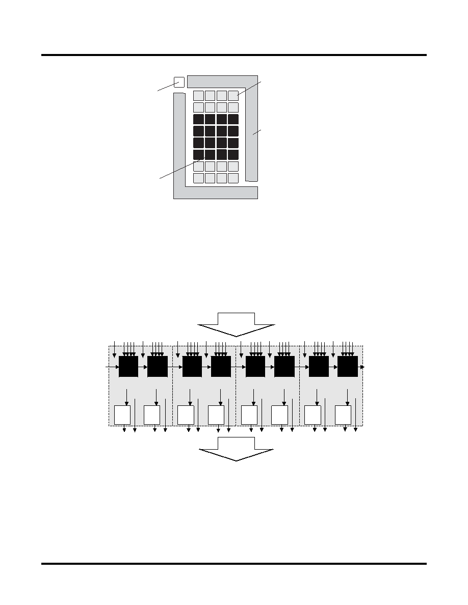
Figure 2-3. Top View of the MachXO256 Device
PFU Blocks
The core of the MachXO devices consists of PFU and PFF blocks. The PFUs can be programmed to perform
Logic, Arithmetic, Distributed RAM, and Distributed ROM functions. PFF blocks can be programmed to perform
Logic, Arithmetic, and Distributed ROM functions. Except where necessary, the remainder of this data sheet will
use the term PFU to refer to both PFU and PFF blocks.
Each PFU block consists of four interconnected Slices, numbered 0-3 as shown in Figure 2-4. There are 53 inputs
and 25 outputs associated with each PFU block.
Figure 2-4. PFU Diagram
Slice
Each Slice contains two LUT4 lookup tables feeding two registers (programmed to be in FF or Latch mode), and
some associated logic that allows the LUTs to be combined to perform functions such as LUT5, LUT6, LUT7, and
LUT8. There is control logic to perform set/reset functions (programmable as synchronous/asynchronous), clock
select, chip-select, and wider RAM/ROM functions. Figure 2-5 shows an overview of the internal logic of the Slice.
The registers in the Slice can be configured for positive/negative and edge/level clocks.
JTAG Port
Programmable
Function
Units with
RAM (PFUs)
Programmable Function
Units without RAM (PFFs)
PIOs Arranged
into sysIO Banks
Slice 0
LUT4 &
CARRY
LUT4 &
CARRY
FF/
Latch
FCIN
FCO
D
FF/
Latch
D
Slice 1
LUT4 &
CARRY
LUT4 &
CARRY
Slice 2
LUT4 &
CARRY
LUT4 &
CARRY
From
Routing
To
Routing
Slice 3
LUT4 &
CARRY
LUT4 &
CARRY
FF/
Latch
D
FF/
Latch
D
FF/
Latch
D
FF/
Latch
D
FF/
Latch
D
FF/
Latch
D
相关PDF资料 |
PDF描述 |
|---|---|
| LCMXO2280E-4M132I | |
| LCMXO2280E-3FT324C | |
| LCMXO2280E-3T144C | |
| LCMXO640C-5T144C | |
| LCMXO2280C-4T100C | |
相关代理商/技术参数 |
参数描述 |
|---|---|
| LCMXO256C-5TN100C | 功能描述:CPLD - 复杂可编程逻辑器件 256 LUTS 78 I/O RoHS:否 制造商:Lattice 系列: 存储类型:EEPROM 大电池数量:128 最大工作频率:333 MHz 延迟时间:2.7 ns 可编程输入/输出端数量:64 工作电源电压:3.3 V 最大工作温度:+ 90 C 最小工作温度:0 C 封装 / 箱体:TQFP-100 |
| LCMXO256C-S-EV | 功能描述:可编程逻辑 IC 开发工具 Eval Board for MachXO RoHS:否 制造商:Altera Corporation 产品:Development Kits 类型:FPGA 工具用于评估:5CEFA7F3 接口类型: 工作电源电压: |
| LCMXO256C-S-EVN | 功能描述:开发软件 MachXO 256 Starter Eval Board RoHS:否 制造商:Atollic Inc. 产品:Compilers/Debuggers 用于:ARM7, ARM9, Cortex-A, Cortex-M, Cortex-R Processors |
| LCMXO256E-3M100C | 功能描述:CPLD - 复杂可编程逻辑器件 256 LUTs 78 IO 1.2V -3 Spd RoHS:否 制造商:Lattice 系列: 存储类型:EEPROM 大电池数量:128 最大工作频率:333 MHz 延迟时间:2.7 ns 可编程输入/输出端数量:64 工作电源电压:3.3 V 最大工作温度:+ 90 C 最小工作温度:0 C 封装 / 箱体:TQFP-100 |
| LCMXO256E-3M100I | 功能描述:CPLD - 复杂可编程逻辑器件 256 LUTs 78 IO 1.2V -3 Spd I RoHS:否 制造商:Lattice 系列: 存储类型:EEPROM 大电池数量:128 最大工作频率:333 MHz 延迟时间:2.7 ns 可编程输入/输出端数量:64 工作电源电压:3.3 V 最大工作温度:+ 90 C 最小工作温度:0 C 封装 / 箱体:TQFP-100 |
发布紧急采购,3分钟左右您将得到回复。