- 您现在的位置:买卖IC网 > PDF目录19832 > LCMXO640C-4M132I (Lattice Semiconductor Corporation)IC PLD 640LUTS 101I/O 132-BGA PDF资料下载
参数资料
| 型号: | LCMXO640C-4M132I |
| 厂商: | Lattice Semiconductor Corporation |
| 文件页数: | 14/88页 |
| 文件大小: | 0K |
| 描述: | IC PLD 640LUTS 101I/O 132-BGA |
| 标准包装: | 360 |
| 系列: | MachXO |
| 可编程类型: | 系统内可编程 |
| 最大延迟时间 tpd(1): | 4.2ns |
| 电压电源 - 内部: | 1.71 V ~ 3.465 V |
| 宏单元数: | 320 |
| 输入/输出数: | 101 |
| 工作温度: | -40°C ~ 100°C |
| 安装类型: | 表面贴装 |
| 封装/外壳: | 132-LFBGA,CSPBGA |
| 供应商设备封装: | 132-CSPBGA(8x8) |
| 包装: | 托盘 |
第1页第2页第3页第4页第5页第6页第7页第8页第9页第10页第11页第12页第13页当前第14页第15页第16页第17页第18页第19页第20页第21页第22页第23页第24页第25页第26页第27页第28页第29页第30页第31页第32页第33页第34页第35页第36页第37页第38页第39页第40页第41页第42页第43页第44页第45页第46页第47页第48页第49页第50页第51页第52页第53页第54页第55页第56页第57页第58页第59页第60页第61页第62页第63页第64页第65页第66页第67页第68页第69页第70页第71页第72页第73页第74页第75页第76页第77页第78页第79页第80页第81页第82页第83页第84页第85页第86页第87页第88页
�� �
�
�Architecture�
�MachXO� Family� Data� Sheet�
�Bus� Size� Matching�
�All� of� the� multi-port� memory� modes� support� different� widths� on� each� of� the� ports.� The� RAM� bits� are� mapped� LSB�
�word� 0� to� MSB� word� 0,� LSB� word� 1� to� MSB� word� 1� and� so� on.� Although� the� word� size� and� number� of� words� for�
�each� port� varies,� this� mapping� scheme� applies� to� each� port.�
�RAM� Initialization� and� ROM� Operation�
�If� desired,� the� contents� of� the� RAM� can� be� pre-loaded� during� device� configuration.� By� preloading� the� RAM� block�
�during� the� chip� configuration� cycle� and� disabling� the� write� controls,� the� sysMEM� block� can� also� be� utilized� as� a�
�ROM.�
�Memory� Cascading�
�Larger� and� deeper� blocks� of� RAMs� can� be� created� using� EBR� sysMEM� Blocks.� Typically,� the� Lattice� design� tools�
�cascade� memory� transparently,� based� on� specific� design� inputs.�
�Single,� Dual,� Pseudo-Dual� Port� and� FIFO� Modes�
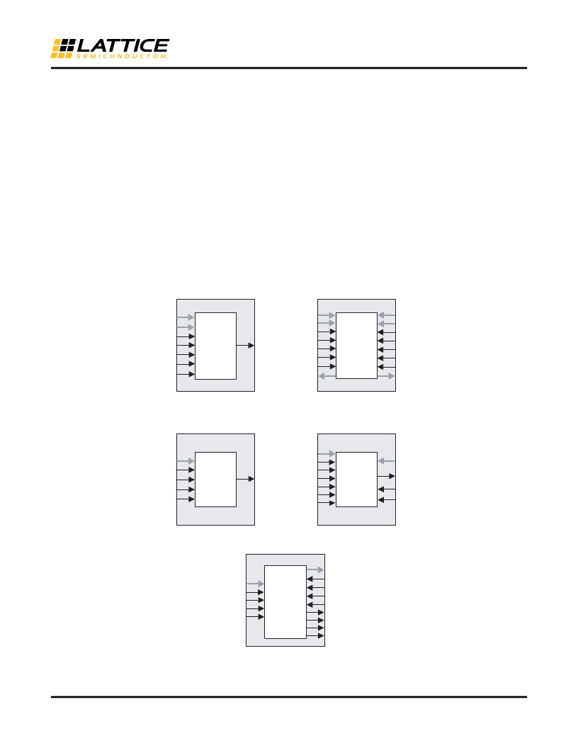
�Figure� 2-12� shows� the� five� basic� memory� configurations� and� their� input/output� names.� In� all� the� sysMEM� RAM�
�modes,� the� input� data� and� address� for� the� ports� are� registered� at� the� input� of� the� memory� array.� The� output� data� of�
�the� memory� is� optionally� registered� at� the� memory� array� output.�
�Figure� 2-12.� sysMEM� Memory� Primitives�
�AD[12:0]�
�DI[35:0]�
�CLK�
�CE�
�RST�
�EBR�
�DO[35:0]�
�ADA[12:0]�
�DIA[17:0]�
�CLKA�
�CEA�
�RSTA�
�WEA�
�EBR�
�ADB[12:0]�
�DIB[17:0]�
�CEB�
�CLKB�
�RSTB�
�WEB�
�WE�
�CS[2:0]�
�AD[12:0]�
�Single� Port� RAM�
�CSA[2:0]�
�DOA[17:0]�
�ADW[12:0]�
�DI[35:0]�
�True� Dual� Port� RAM�
�CSB[2:0]�
�DOB[17:0]�
�ADR[12:0]�
�CLK�
�CE�
�RST�
�CS[2:0]�
�EBR�
�DO[35:0]�
�CLKW�
�CEW�
�WE�
�RST�
�CS[2:0]�
�EBR�
�DO[35:0]�
�CER�
�CLKR�
�ROM�
�Pseudo-Dual� Port� RAM�
�DO[35:0]�
�DI[35:0]�
�CLKW�
�RSTA�
�WE�
�CEW�
�EBR�
�CLKR�
�RSTB�
�RE�
�RCE�
�FF�
�AF�
�EF�
�AE�
�FIFO�
�2-11�
�相关PDF资料 |
PDF描述 |
|---|---|
| RMA35DRSI-S288 | CONN EDGECARD 70POS .125 EXTEND |
| LLL317R70J225MA01L | CAP CER 2.2UF 6.3V 20% X7R 0612 |
| LCMXO640E-4MN132I | IC FPGA 640LUTS 132CSBGA |
| GCM18DCMD | CONN EDGECARD 36POS .156 WW |
| 10018784-11002TLF | CONN PCI EXPRESS 98POS VERT PCB |
相关代理商/技术参数 |
参数描述 |
|---|---|
| LCMXO640C-4MN100C | 功能描述:CPLD - 复杂可编程逻辑器件 640 LUTs 74 IO 1.8/2 .5/3.3V -4 Spd RoHS:否 制造商:Lattice 系列: 存储类型:EEPROM 大电池数量:128 最大工作频率:333 MHz 延迟时间:2.7 ns 可编程输入/输出端数量:64 工作电源电压:3.3 V 最大工作温度:+ 90 C 最小工作温度:0 C 封装 / 箱体:TQFP-100 |
| LCMXO640C-4MN100I | 功能描述:CPLD - 复杂可编程逻辑器件 640 LUTs 74 IO 1.8/2 .5/3.3V -4 Spd I RoHS:否 制造商:Lattice 系列: 存储类型:EEPROM 大电池数量:128 最大工作频率:333 MHz 延迟时间:2.7 ns 可编程输入/输出端数量:64 工作电源电压:3.3 V 最大工作温度:+ 90 C 最小工作温度:0 C 封装 / 箱体:TQFP-100 |
| LCMXO640C-4MN132C | 功能描述:CPLD - 复杂可编程逻辑器件 640 LUTs 101 I/O 1.8/2.5/3.3V -4 Spd RoHS:否 制造商:Lattice 系列: 存储类型:EEPROM 大电池数量:128 最大工作频率:333 MHz 延迟时间:2.7 ns 可编程输入/输出端数量:64 工作电源电压:3.3 V 最大工作温度:+ 90 C 最小工作温度:0 C 封装 / 箱体:TQFP-100 |
| LCMXO640C-4MN132I | 功能描述:CPLD - 复杂可编程逻辑器件 640 LUTs 101 IO 1.8/ 2.5/3.3V -4 Spd I RoHS:否 制造商:Lattice 系列: 存储类型:EEPROM 大电池数量:128 最大工作频率:333 MHz 延迟时间:2.7 ns 可编程输入/输出端数量:64 工作电源电压:3.3 V 最大工作温度:+ 90 C 最小工作温度:0 C 封装 / 箱体:TQFP-100 |
| LCMXO640C-4T100C | 功能描述:CPLD - 复杂可编程逻辑器件 640 LUTs 74 IO 1.8/2 .5/3.3V -4 Spd RoHS:否 制造商:Lattice 系列: 存储类型:EEPROM 大电池数量:128 最大工作频率:333 MHz 延迟时间:2.7 ns 可编程输入/输出端数量:64 工作电源电压:3.3 V 最大工作温度:+ 90 C 最小工作温度:0 C 封装 / 箱体:TQFP-100 |
发布紧急采购,3分钟左右您将得到回复。