- 您现在的位置:买卖IC网 > PDF目录177783 > LCMXO640C-5T100C (LATTICE SEMICONDUCTOR CORP) PDF资料下载
参数资料
| 型号: | LCMXO640C-5T100C |
| 厂商: | LATTICE SEMICONDUCTOR CORP |
| 元件分类: | PLD |
| 中文描述: | FLASH PLD, 3.5 ns, PQFP100 |
| 封装: | 14 X 14 MM, TQFP-100 |
| 文件页数: | 35/96页 |
| 文件大小: | 1389K |
| 代理商: | LCMXO640C-5T100C |
第1页第2页第3页第4页第5页第6页第7页第8页第9页第10页第11页第12页第13页第14页第15页第16页第17页第18页第19页第20页第21页第22页第23页第24页第25页第26页第27页第28页第29页第30页第31页第32页第33页第34页当前第35页第36页第37页第38页第39页第40页第41页第42页第43页第44页第45页第46页第47页第48页第49页第50页第51页第52页第53页第54页第55页第56页第57页第58页第59页第60页第61页第62页第63页第64页第65页第66页第67页第68页第69页第70页第71页第72页第73页第74页第75页第76页第77页第78页第79页第80页第81页第82页第83页第84页第85页第86页第87页第88页第89页第90页第91页第92页第93页第94页第95页第96页
3-14
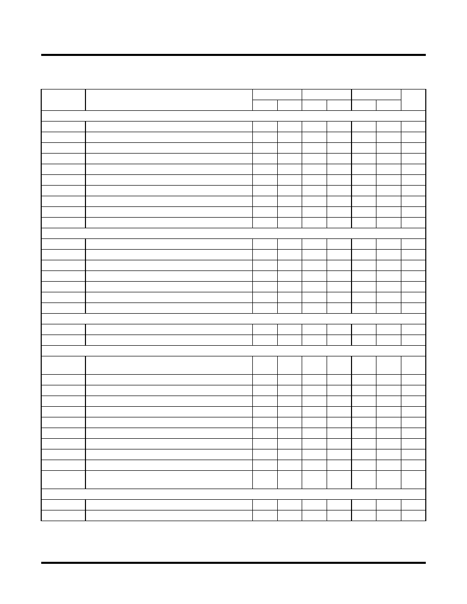
DC and Switching Characteristics
Lattice Semiconductor
MachXO Family Data Sheet
MachXO Internal Timing Parameters
1
Over Recommended Operating Conditions
Parameter
Description
-5
-4
-3
Units
Min.
Max.
Min.
Max.
Min.
Max.
PFU/PFF Logic Mode Timing
tLUT4_PFU
LUT4 delay (A to D inputs to F output)
—
0.28
—
0.34
—
0.39
ns
tLUT6_PFU
LUT6 delay (A to D inputs to OFX output)
—
0.44
—
0.53
—
0.62
ns
tLSR_PFU
Set/Reset to output of PFU
—
0.90
—
1.08
—
1.26
ns
tSUM_PFU
Clock to Mux (M0,M1) input setup time
0.10
—
0.13
—
0.15
—
ns
tHM_PFU
Clock to Mux (M0,M1) input hold time
-0.05
—
-0.06
—
-0.07
—
ns
tSUD_PFU
Clock to D input setup time
0.13
—
0.16
—
0.18
—
ns
tHD_PFU
Clock to D input hold time
-0.03
—
-0.03
—
-0.04
—
ns
tCK2Q_PFU
Clock to Q delay, D-type register configuration
—
0.40
—
0.48
—
0.56
ns
tLE2Q_PFU
Clock to Q delay latch configuration
—
0.53
—
0.64
—
0.74
ns
tLD2Q_PFU
D to Q throughput delay when latch is enabled
—
0.55
—
0.66
—
0.77
ns
PFU Dual Port Memory Mode Timing
tCORAM_PFU
Clock to Output
—
0.40
—
0.48
—
0.56
ns
tSUDATA_PFU Data Setup Time
-0.18
—
-0.22
—
-0.25
—
ns
tHDATA_PFU
Data Hold Time
0.28
—
0.34
—
0.39
—
ns
tSUADDR_PFU Address Setup Time
-0.46
—
-0.56
—
-0.65
—
ns
tHADDR_PFU
Address Hold Time
0.71
—
0.85
—
0.99
—
ns
tSUWREN_PFU Write/Read Enable Setup Time
-0.22
—
-0.26
—
-0.30
—
ns
tHWREN_PFU Write/Read Enable Hold Time
0.33
—
0.40
—
0.47
—
ns
PIO Input/Output Buffer Timing
tIN_PIO
Input Buffer Delay
—
0.75
—
0.90
—
1.06
ns
tOUT_PIO
Output Buffer Delay
—
1.29
—
1.54
—
1.80
ns
EBR Timing (1200 and 2280 Devices Only)
tCO_EBR
Clock to output from Address or Data with no output
register
—
2.24
—
2.69
—
3.14
ns
tCOO_EBR
Clock to output from EBR output Register
—
0.54
—
0.64
—
0.75
ns
tSUDATA_EBR Setup Data to EBR Memory
-0.26
—
-0.31
—
-0.37
—
ns
tHDATA_EBR
Hold Data to EBR Memory
0.41
—
0.49
—
0.57
—
ns
tSUADDR_EBR Setup Address to EBR Memory
-0.26
—
-0.31
—
-0.37
—
ns
tHADDR_EBR
Hold Address to EBR Memory
0.41
—
0.49
—
0.57
—
ns
tSUWREN_EBR Setup Write/Read Enable to EBR Memory
-0.17
—
-0.20
—
-0.23
—
ns
tHWREN_EBR Hold Write/Read Enable to EBR Memory
0.26
—
0.31
—
0.36
—
ns
tSUCE_EBR
Clock Enable Setup Time to EBR Output Register
0.19
—
0.23
—
0.27
—
ns
tHCE_EBR
Clock Enable Hold Time to EBR Output Register
-0.13
—
-0.16
—
-0.18
—
ns
tRSTO_EBR
Reset To Output Delay Time from EBR Output Regis-
ter
—
1.03
—
1.23
—
1.44
ns
PLL Parameters (1200 and 2280 Devices Only)
tRSTREC
Reset Recovery to Rising Clock
1.00
—
1.00
—
1.00
—
ns
tRSTSU
Reset Signal Setup Time
1.00
—
1.00
—
1.00
—
ns
1. Internal parameters are characterized but not tested on every device.
Rev. A 0.19
相关PDF资料 |
PDF描述 |
|---|---|
| LCMXO2280E-4T100I | |
| LCMXO2280C-5FT324C | |
| LCMXO2280E-4FT256I | |
| LCMXO2280E-3FT256C | |
| LCMXO640C-4T100C | |
相关代理商/技术参数 |
参数描述 |
|---|---|
| LCMXO640C-5T144C | 功能描述:CPLD - 复杂可编程逻辑器件 640 LUTS 113 I/O RoHS:否 制造商:Lattice 系列: 存储类型:EEPROM 大电池数量:128 最大工作频率:333 MHz 延迟时间:2.7 ns 可编程输入/输出端数量:64 工作电源电压:3.3 V 最大工作温度:+ 90 C 最小工作温度:0 C 封装 / 箱体:TQFP-100 |
| LCMXO640C-5TN100C | 功能描述:CPLD - 复杂可编程逻辑器件 640 LUTS 74 I/O RoHS:否 制造商:Lattice 系列: 存储类型:EEPROM 大电池数量:128 最大工作频率:333 MHz 延迟时间:2.7 ns 可编程输入/输出端数量:64 工作电源电压:3.3 V 最大工作温度:+ 90 C 最小工作温度:0 C 封装 / 箱体:TQFP-100 |
| LCMXO640C-5TN100C4W | 制造商:Lattice Semiconductor Corporation 功能描述:MACHXO PLD FLASH SCRAM 1.8V 640 |
| LCMXO640C-5TN144C | 功能描述:CPLD - 复杂可编程逻辑器件 640 LUTS 113 I/O RoHS:否 制造商:Lattice 系列: 存储类型:EEPROM 大电池数量:128 最大工作频率:333 MHz 延迟时间:2.7 ns 可编程输入/输出端数量:64 工作电源电压:3.3 V 最大工作温度:+ 90 C 最小工作温度:0 C 封装 / 箱体:TQFP-100 |
| LCMXO640C-5TN144C4W | 制造商:Lattice Semiconductor Corporation 功能描述:MACHXO PLD FLASH SCRAM 1.8V 640 |
发布紧急采购,3分钟左右您将得到回复。