- 您现在的位置:买卖IC网 > PDF目录19832 > LCMXO640E-5MN132C (Lattice Semiconductor Corporation)IC FPGA 640LUTS 132CSBGA PDF资料下载
参数资料
| 型号: | LCMXO640E-5MN132C |
| 厂商: | Lattice Semiconductor Corporation |
| 文件页数: | 17/88页 |
| 文件大小: | 0K |
| 描述: | IC FPGA 640LUTS 132CSBGA |
| 标准包装: | 360 |
| 系列: | MachXO |
| 可编程类型: | 系统内可编程 |
| 最大延迟时间 tpd(1): | 3.5ns |
| 电压电源 - 内部: | 1.14 V ~ 1.26 V |
| 宏单元数: | 320 |
| 输入/输出数: | 101 |
| 工作温度: | 0°C ~ 85°C |
| 安装类型: | 表面贴装 |
| 封装/外壳: | 132-LFBGA,CSPBGA |
| 供应商设备封装: | 132-CSPBGA(8x8) |
| 包装: | 托盘 |
第1页第2页第3页第4页第5页第6页第7页第8页第9页第10页第11页第12页第13页第14页第15页第16页当前第17页第18页第19页第20页第21页第22页第23页第24页第25页第26页第27页第28页第29页第30页第31页第32页第33页第34页第35页第36页第37页第38页第39页第40页第41页第42页第43页第44页第45页第46页第47页第48页第49页第50页第51页第52页第53页第54页第55页第56页第57页第58页第59页第60页第61页第62页第63页第64页第65页第66页第67页第68页第69页第70页第71页第72页第73页第74页第75页第76页第77页第78页第79页第80页第81页第82页第83页第84页第85页第86页第87页第88页
�� �
�
�Architecture�
�MachXO� Family� Data� Sheet�
�PIO� Groups�
�On� the� MachXO� devices,� PIO� cells� are� assembled� into� two� different� types� of� PIO� groups,� those� with� four� PIO� cells�
�and� those� with� six� PIO� cells.� PIO� groups� with� four� IOs� are� placed� on� the� left� and� right� sides� of� the� device� while� PIO�
�groups� with� six� IOs� are� placed� on� the� top� and� bottom.� The� individual� PIO� cells� are� connected� to� their� respective�
�sysIO� buffers� and� PADs.�
�On� all� MachXO� devices,� two� adjacent� PIOs� can� be� joined� to� provide� a� complementary� Output� driver� pair.� The� I/O�
�pin� pairs� are� labeled� as� "T"� and� "C"� to� distinguish� between� the� true� and� complement� pins.�
�The� MachXO1200� and� MachXO2280� devices� contain� enhanced� I/O� capability.� All� PIO� pairs� on� these� larger�
�devices� can� implement� differential� receivers.� In� addition,� half� of� the� PIO� pairs� on� the� left� and� right� sides� of� these�
�devices� can� be� configured� as� LVDS� transmit/receive� pairs.� PIOs� on� the� top� of� these� larger� devices� also� provide� PCI�
�support.�
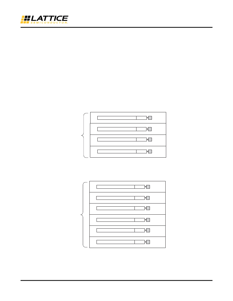
�Figure� 2-15.� Group� of� Four� Programmable� I/O� Cells�
�This� structure� is� used� on� the�
�left� and� right� of� MachXO� devices�
�PIO� A�
�PIO� B�
�Four� PIOs�
�PIO� C�
�PIO� D�
�Figure� 2-16.� Group� oftSix� Programmable� I/O� Cells�
�This� structure� is� used� on� the� top�
�and� bottom� of� MachXO� devices�
�PIO� A�
�PIO� B�
�PIO� C�
�Six� PIOs�
�PIO� D�
�PIO� E�
�PIO� F�
�PADA� "T"�
�PADB� "C"�
�PADC� "T"�
�PADD� "C"�
�PADA� "T"�
�PADB� "C"�
�PADC� "T"�
�PADD� "C"�
�PADE� "T"�
�PADF� "C"�
�PIO�
�The� PIO� blocks� provide� the� interface� between� the� sysIO� buffers� and� the� internal� PFU� array� blocks.� These� blocks�
�receive� output� data� from� the� PFU� array� and� a� fast� output� data� signal� from� adjacent� PFUs.� The� output� data� and� fast�
�2-14�
�相关PDF资料 |
PDF描述 |
|---|---|
| RBM12DSEH | CONN EDGECARD 24POS .156 EYELET |
| LTC1647-2IS8#TR | IC CONTROLLER HOTSWAP DUAL 8SOIC |
| LCMXO640C-5MN132C | IC PLD 640LUTS 101I/O 132-BGA |
| RMA36DRMN-S288 | CONN EDGECARD 72POS .125 EXTEND |
| GCA18DRMN | CONN EDGECARD 36POS .125 SQ WW |
相关代理商/技术参数 |
参数描述 |
|---|---|
| LCMXO640E-5T100C | 功能描述:CPLD - 复杂可编程逻辑器件 640 LUTs 74 IO 1.2V -5 Spd RoHS:否 制造商:Lattice 系列: 存储类型:EEPROM 大电池数量:128 最大工作频率:333 MHz 延迟时间:2.7 ns 可编程输入/输出端数量:64 工作电源电压:3.3 V 最大工作温度:+ 90 C 最小工作温度:0 C 封装 / 箱体:TQFP-100 |
| LCMXO640E-5T144C | 功能描述:CPLD - 复杂可编程逻辑器件 640 LUTs 113 IO 1.2V -5 Spd RoHS:否 制造商:Lattice 系列: 存储类型:EEPROM 大电池数量:128 最大工作频率:333 MHz 延迟时间:2.7 ns 可编程输入/输出端数量:64 工作电源电压:3.3 V 最大工作温度:+ 90 C 最小工作温度:0 C 封装 / 箱体:TQFP-100 |
| LCMXO640E-5TN100C | 功能描述:CPLD - 复杂可编程逻辑器件 640 LUTs 74 IO 1.2V -5 Spd RoHS:否 制造商:Lattice 系列: 存储类型:EEPROM 大电池数量:128 最大工作频率:333 MHz 延迟时间:2.7 ns 可编程输入/输出端数量:64 工作电源电压:3.3 V 最大工作温度:+ 90 C 最小工作温度:0 C 封装 / 箱体:TQFP-100 |
| LCMXO640E-5TN144C | 功能描述:CPLD - 复杂可编程逻辑器件 640 LUTs 113 IO 1.2V -5 Spd RoHS:否 制造商:Lattice 系列: 存储类型:EEPROM 大电池数量:128 最大工作频率:333 MHz 延迟时间:2.7 ns 可编程输入/输出端数量:64 工作电源电压:3.3 V 最大工作温度:+ 90 C 最小工作温度:0 C 封装 / 箱体:TQFP-100 |
| LCMXO640LUTSC-3FT256C | 制造商:LATTICE 制造商全称:Lattice Semiconductor 功能描述:MachXO Family Data Sheet |
发布紧急采购,3分钟左右您将得到回复。