- 您现在的位置:买卖IC网 > PDF目录4587 > LFEC6E-5QN208C (Lattice Semiconductor Corporation)IC FPGA 6.1KLUTS 147I/O 208-PQFP PDF资料下载
参数资料
| 型号: | LFEC6E-5QN208C |
| 厂商: | Lattice Semiconductor Corporation |
| 文件页数: | 35/163页 |
| 文件大小: | 0K |
| 描述: | IC FPGA 6.1KLUTS 147I/O 208-PQFP |
| 标准包装: | 24 |
| 系列: | EC |
| 逻辑元件/单元数: | 6100 |
| RAM 位总计: | 94208 |
| 输入/输出数: | 147 |
| 电源电压: | 1.14 V ~ 1.26 V |
| 安装类型: | 表面贴装 |
| 工作温度: | 0°C ~ 85°C |
| 封装/外壳: | 208-BFQFP |
| 供应商设备封装: | 208-PQFP(28x28) |
第1页第2页第3页第4页第5页第6页第7页第8页第9页第10页第11页第12页第13页第14页第15页第16页第17页第18页第19页第20页第21页第22页第23页第24页第25页第26页第27页第28页第29页第30页第31页第32页第33页第34页当前第35页第36页第37页第38页第39页第40页第41页第42页第43页第44页第45页第46页第47页第48页第49页第50页第51页第52页第53页第54页第55页第56页第57页第58页第59页第60页第61页第62页第63页第64页第65页第66页第67页第68页第69页第70页第71页第72页第73页第74页第75页第76页第77页第78页第79页第80页第81页第82页第83页第84页第85页第86页第87页第88页第89页第90页第91页第92页第93页第94页第95页第96页第97页第98页第99页第100页第101页第102页第103页第104页第105页第106页第107页第108页第109页第110页第111页第112页第113页第114页第115页第116页第117页第118页第119页第120页第121页第122页第123页第124页第125页第126页第127页第128页第129页第130页第131页第132页第133页第134页第135页第136页第137页第138页第139页第140页第141页第142页第143页第144页第145页第146页第147页第148页第149页第150页第151页第152页第153页第154页第155页第156页第157页第158页第159页第160页第161页第162页第163页
2-10
Architecture
LatticeECP/EC Family Data Sheet
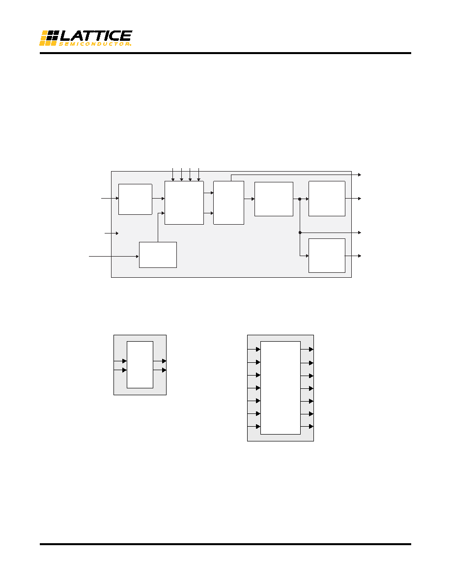
grammed during configuration or can be adjusted dynamically. In dynamic mode, the PLL may lose lock after
adjustment and not relock until the tLOCK parameter has been satisfied. Additionally, the phase and duty cycle block
allows the user to adjust the phase and duty cycle of the CLKOS output.
The sysCLOCK PLLs provide the ability to synthesize clock frequencies. Each PLL has four dividers associated
with it: input clock divider, feedback divider, post scalar divider and secondary clock divider. The input clock divider
is used to divide the input clock signal, while the feedback divider is used to multiply the input clock signal. The post
scalar divider allows the VCO to operate at higher frequencies than the clock output, thereby increasing the fre-
quency range. The secondary divider is used to derive lower frequency outputs.
Figure 2-11. PLL Diagram
Figure 2-12 shows the available macros for the PLL. Table 2-5 provides signal description of the PLL Block.
Figure 2-12. PLL Primitive
VCO
CLKOS
CLKOK
LOCK
RST
CLKFB
from CLKOP
(PLL internal),
from clock net
(CLKOP) or
from a user
clock (PIN or logic)
Dynamic Delay Adjustment
Input Clock
Divider
(CLKI)
Feedback
Divider
(CLKFB)
Post Scalar
Divider
(CLKOP)
Phase/Duty
Select
Secondary
Clock
Divider
(CLKOK)
Delay
Adjust
Voltage
Controlled
Oscillator
CLKI
(from routing or
external pin)
CLKOP
EPLLB
CLKOP
CLKI
CLKFB
LOCK
EHXPLLB
CLKOS
CLKI
CLKFB
CLKOK
LOCK
RST
CLKOP
DDAIZR
DDAILAG
DDA MODE
DDAIDEL[2:0]
DDAOZR
DDAOLAG
DDAODEL[2:0]
相关PDF资料 |
PDF描述 |
|---|---|
| MIC5310-NKYML TR | IC REG LDO 2.85V/2.6V .15A 8-MLF |
| LT1963AMPS8#PBF | IC REG LDO ADJ 1.5A 8-SOIC |
| MIC5310-NDYML TR | IC REG LDO 2.85/1.85V .15A 8-MLF |
| RMA43DTAH | CONN EDGECARD 86POS R/A .125 SLD |
| RSA43DTAD | CONN EDGECARD 86POS R/A .125 SLD |
相关代理商/技术参数 |
参数描述 |
|---|---|
| LFEC6E-5QN208I | 制造商:LATTICE 制造商全称:Lattice Semiconductor 功能描述:LatticeECP/EC Family Data Sheet |
| LFEC6E-5T100C | 制造商:LATTICE 制造商全称:Lattice Semiconductor 功能描述:LatticeECP/EC Family Data Sheet |
| LFEC6E-5T100I | 制造商:LATTICE 制造商全称:Lattice Semiconductor 功能描述:LatticeECP/EC Family Data Sheet |
| LFEC6E-5T144C | 功能描述:FPGA - 现场可编程门阵列 6.1 LUT 97 I/O RoHS:否 制造商:Altera Corporation 系列:Cyclone V E 栅极数量: 逻辑块数量:943 内嵌式块RAM - EBR:1956 kbit 输入/输出端数量:128 最大工作频率:800 MHz 工作电源电压:1.1 V 最大工作温度:+ 70 C 安装风格:SMD/SMT 封装 / 箱体:FBGA-256 |
| LFEC6E-5T144I | 制造商:LATTICE 制造商全称:Lattice Semiconductor 功能描述:LatticeECP/EC Family Data Sheet |
发布紧急采购,3分钟左右您将得到回复。