- 您现在的位置:买卖IC网 > PDF目录299403 > LFXP20E-5FN484C (LATTICE SEMICONDUCTOR CORP) PDF资料下载
参数资料
| 型号: | LFXP20E-5FN484C |
| 厂商: | LATTICE SEMICONDUCTOR CORP |
| 元件分类: | FPGA |
| 中文描述: | FPGA, 2464 CLBS, PBGA484 |
| 封装: | 23 X 23 MM, LEAD FREE, FPBGA-484 |
| 文件页数: | 45/130页 |
| 文件大小: | 1312K |
| 代理商: | LFXP20E-5FN484C |
第1页第2页第3页第4页第5页第6页第7页第8页第9页第10页第11页第12页第13页第14页第15页第16页第17页第18页第19页第20页第21页第22页第23页第24页第25页第26页第27页第28页第29页第30页第31页第32页第33页第34页第35页第36页第37页第38页第39页第40页第41页第42页第43页第44页当前第45页第46页第47页第48页第49页第50页第51页第52页第53页第54页第55页第56页第57页第58页第59页第60页第61页第62页第63页第64页第65页第66页第67页第68页第69页第70页第71页第72页第73页第74页第75页第76页第77页第78页第79页第80页第81页第82页第83页第84页第85页第86页第87页第88页第89页第90页第91页第92页第93页第94页第95页第96页第97页第98页第99页第100页第101页第102页第103页第104页第105页第106页第107页第108页第109页第110页第111页第112页第113页第114页第115页第116页第117页第118页第119页第120页第121页第122页第123页第124页第125页第126页第127页第128页第129页第130页
2-18
Architecture
Lattice Semiconductor
LatticeXP Family Data Sheet
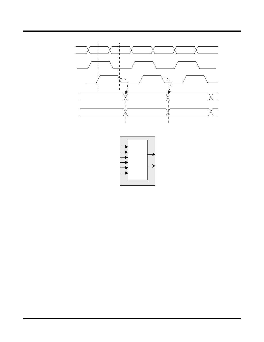
Figure 2-21. Input Register DDR Waveforms
Figure 2-22. INDDRXB Primitive
Output Register Block
The output register block provides the ability to register signals from the core of the device before they are passed
to the sysIO buffers. The block contains a register for SDR operation that is combined with an additional latch for
DDR operation. Figure 2-23 shows the diagram of the Output Register Block.
In SDR mode, ONEG0 feeds one of the flip-flops that then feeds the output. The flip-flop can be configured as a D-
type or as a latch. In DDR mode, ONEG0 is fed into one register on the positive edge of the clock and OPOS0 is
latched. A multiplexer running off the same clock selects the correct register for feeding to the output (D0).
Figure 2-24 shows the design tool DDR primitives. The SDR output register has reset and clock enable available.
The additional register for DDR operation does not have reset or clock enable available.
AB
C
D
E
F
BD
DI
(In DDR Mode)
D0
D2
DQS
A
C
DQS
Delayed
IDDRXB
LSR
QA
D
ECLK
QB
DDRCLKPOL
SCLK
CE
相关PDF资料 |
PDF描述 |
|---|---|
| LFXP15C-4FN256C | |
| LFZ3508VXX | GENERAL PURPOSE INDUCTOR |
| LFZ2805HXX | GENERAL PURPOSE INDUCTOR |
| LF02004VTX | GENERAL PURPOSE INDUCTOR |
| LG3341-NE7501 | T-1 SINGLE COLOR LED, GREEN, 3 mm |
相关代理商/技术参数 |
参数描述 |
|---|---|
| LFXP217E5CF484C | 制造商:LATTICE 制造商全称:Lattice Semiconductor 功能描述:LatticeXP2 Family Data Sheet |
| LFXP217E5CF484I | 制造商:LATTICE 制造商全称:Lattice Semiconductor 功能描述:LatticeXP2 Family Data Sheet |
| LFXP217E5CF672C | 制造商:LATTICE 制造商全称:Lattice Semiconductor 功能描述:LatticeXP2 Family Data Sheet |
| LFXP217E5CF672I | 制造商:LATTICE 制造商全称:Lattice Semiconductor 功能描述:LatticeXP2 Family Data Sheet |
| LFXP217E5CFN484C | 制造商:LATTICE 制造商全称:Lattice Semiconductor 功能描述:LatticeXP2 Family Data Sheet |
发布紧急采购,3分钟左右您将得到回复。