- 您现在的位置:买卖IC网 > PDF目录43920 > LIT1108CS8-12#PBF (LINEAR TECHNOLOGY CORP) 1.5 A SWITCHING REGULATOR, 25 kHz SWITCHING FREQ-MAX, PDSO8 PDF资料下载
参数资料
| 型号: | LIT1108CS8-12#PBF |
| 厂商: | LINEAR TECHNOLOGY CORP |
| 元件分类: | 稳压器 |
| 英文描述: | 1.5 A SWITCHING REGULATOR, 25 kHz SWITCHING FREQ-MAX, PDSO8 |
| 封装: | PLASTIC, SOIC-8 |
| 文件页数: | 12/12页 |
| 文件大小: | 266K |
| 代理商: | LIT1108CS8-12#PBF |
9
LT1108
U
S
A
O
PPLICATI
WU
U
I FOR ATIO
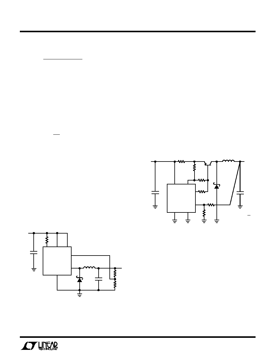
HIGHER CURRENT STEP-DOWN OPERATION
Output current can be increased by using a discrete PNP
pass transistor as shown in Figure 3. R1 serves as a
current limit sense. When the voltage drop across R1
equals 0.5VBE, the switch turns off. As shown, switch
current is limited to 2A. Inductor value can be calculated
based on formulas in the Inductor Selection Step-Down
Converter section with the following conservative expres-
sion for VSW:
VV
V
SW
R
Q SAT
=+
≈
11
10
24
.(
)
R2 provides a current path to turn off Q1. R3 provides base
drive to Q1. R4 and R5 set output voltage. A PMOS FET can
be used in place of Q1 when VIN is between 10V and 20V.
Figure 2. Step-Down Mode Hookup
LT1108 F02
GND
SW2
SW1
ILIM
R3
100
FB
VOUT
+
C2
+
C1
D1
1N5818
VIN
R2
R1
L1
LT1108
VIN
LT1108 F03
D1
1N5821
+
VOUT
VIN
30V
MAX
L1
R1
0.15
R2
100
Q1
ZETEX ZTX749
R3
330
R4
R5
C1
LT1108
GND
SW2
SW1
VIN
IL
FB
C2
R6
100
VOUT = 1.245V 1 +
R4
R5
()
INVERTING CONFIGURATIONS
The LT1108 can be configured as a positive-to-negative
converter (Figure 4), or a negative-to-positive converter
(Figure 5). In Figure 4, the arrangement is very similar to a
step-down, except that the high side of the feedback is
referred to ground. This level shifts the output negative. As
in the step-down mode, D1 must be a Schottky diode,
and
VOUTshould be less than 6.2V. More negative output
voltages can be accommodated as in the prior section.
In Figure 5, the input is negative while the output is positive.
In this configuration, the magnitude of the input voltage can
be higher or lower than the output voltage. A level shift,
I
V
VV
L
t
PEAK
IN
SW
OUT
ON
=
()
22
When the switch turns off, the SW2 pin falls rapidly and
actually goes below ground. D1 turns on when SW2
reaches 0.4V below ground.
D1 MUST BE A SCHOTTKY
DIODE. The voltage at SW2 must never be allowed to go
below –0.5V. A silicon diode such as the 1N4933 will allow
SW2 to go to –0.8V, causing potentially destructive power
dissipation inside the LT1108. Output voltage is deter-
mined by
V
R
V
OUT =+
()
1
2
1
1 245
23
.(
)
R3 programs switch current limit. This is especially impor-
tant in applications where the input varies over a wide
range. Without R3, the switch stays on for a fixed time each
cycle. Under certain conditions the current in L1 can build
up to excessive levels, exceeding the switch rating and/or
saturating the inductor. The 100
resistor programs the
switch to turn off when the current reaches approximately
700mA. When using the LT1108 in step-down mode,
output voltage should be limited to 6.2V or less. Higher
output voltages can be accommodated by inserting a
1N5818 diode in series with the SW2 pin (anode connected
to SW2).
Figure 3. Q1 Permits Higher Current Switching
The LT1108 Functions as Controller
相关PDF资料 |
PDF描述 |
|---|---|
| LK1001-7EDDT | 1-OUTPUT 150 W AC-DC REG PWR SUPPLY MODULE |
| LK1001-7ERD6TB1 | 1-OUTPUT 150 W AC-DC REG PWR SUPPLY MODULE |
| LK1001-7ERD6T | 1-OUTPUT 150 W AC-DC REG PWR SUPPLY MODULE |
| LK1001-7PD0 | 1-OUTPUT 150 W AC-DC REG PWR SUPPLY MODULE |
| LK1001-7RD1T | 1-OUTPUT 150 W AC-DC REG PWR SUPPLY MODULE |
相关代理商/技术参数 |
参数描述 |
|---|---|
| LIT-2013 | 制造商:JST Manufacturing 功能描述: |
| LI-TB01 | 功能描述:开发板和工具包 - ARM DM365 LEOPARDBOARD DEVELOPMENT BOARD RoHS:否 制造商:Arduino 产品:Development Boards 工具用于评估:ATSAM3X8EA-AU 核心:ARM Cortex M3 接口类型:DAC, ICSP, JTAG, UART, USB 工作电源电压:3.3 V |
| LI-TB02 | 功能描述:开发板和工具包 - ARM DM368 LEOPARDBOARD DEVELOPMENT BOARD RoHS:否 制造商:Arduino 产品:Development Boards 工具用于评估:ATSAM3X8EA-AU 核心:ARM Cortex M3 接口类型:DAC, ICSP, JTAG, UART, USB 工作电源电压:3.3 V |
| LIT-DSD-860972-4 | 制造商:PCA 功能描述:LIT-DSD-860972-4 |
| LITERATURE ED 5 | 制造商:SOLA/HEVI-DUTY 功能描述:_ |
发布紧急采购,3分钟左右您将得到回复。