- 您现在的位置:买卖IC网 > PDF目录79893 > LK1001-9PD5TB1 1-OUTPUT 150 W AC-DC REG PWR SUPPLY MODULE PDF资料下载
参数资料
| 型号: | LK1001-9PD5TB1 |
| 元件分类: | 电源模块 |
| 英文描述: | 1-OUTPUT 150 W AC-DC REG PWR SUPPLY MODULE |
| 封装: | METAL, CASE K02, MODULE |
| 文件页数: | 14/27页 |
| 文件大小: | 640K |
| 代理商: | LK1001-9PD5TB1 |
第1页第2页第3页第4页第5页第6页第7页第8页第9页第10页第11页第12页第13页当前第14页第15页第16页第17页第18页第19页第20页第21页第22页第23页第24页第25页第26页第27页
K-Family
DC-DC Converters >100 W
Rugged Environment
8 - 22
Edition 2/96 - Melcher AG
MELCHER
The Power Partners.
8.1
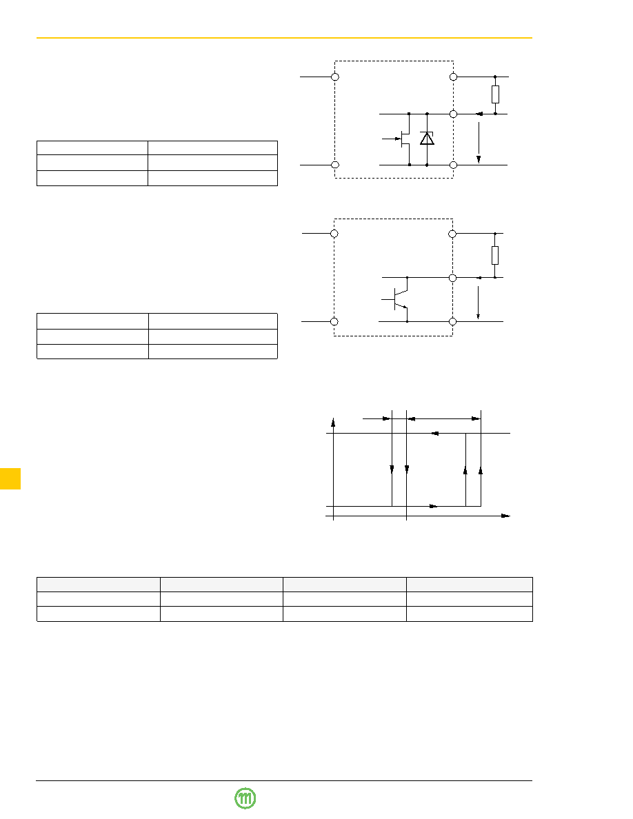
Fig. 24
Option D1...D0: JFET output, ID ≤ 2.5 mA
NPN output (D5...DD):
Connector pin D is internally connected via the collector-
emitter path of a NPN transistor to the negative potential of
output 1.
UD < 0.4 V (logic low) corresponds to a monitored
voltage level (
Ui and/or Uo1) > Ut +Uh. The current ID
through the open collector should not exceed 20 mA. The
NPN output is not protected against external overvoltages.
UD should not exceed 40 V.
Ui, Uo1 status
D output,
UD
Ui or Uo1 < Ut
high, H,
I D ≤ 25 A at UD = 40 V
Ui and Uo1 > Ut + Uh
low, L,
UD
≤ 0.4 V at ID = 20 mA
Threshold tolerances and hysteresis:
If
Ui is monitored, the internal input voltage after the input
filter and rectifier (LK types) is measured. Consequently
this voltage differs from the voltage at the connector pins by
the voltage drop
U
ti across input filter and rectifier. The
threshold levels of the D0 and D9 options are factory ad-
justed at nominal output current
Io nom and at TA = 25 °C. The
value of
U
ti depends upon the input voltage range (CK,
DK, ..), threshold level
Ut, temperature and input current.
The input current is a function of the input voltage and the
output power.
Fig. 26
Definition of Uti, Ut i and Uhi (JFET output)
Table 16: D-output logic signals
Version of D
Ui < Ut resp. Uo < Ut
Ui > Ut + Uh resp. Uo > Ut
Configuration
D1, D2, D3, D4, D0
low
high
JFET
D5, D6, D7, D8, D9, DD
high
low
NPN
JFET output (D0…D4):
Connector pin D is internally connected via the drain-
source path of a JFET (self-conducting type) to the nega-
tive potential of output 1.
UD ≤ 0.4 V (logic low) corresponds
to a monitored voltage level (
Ui and/or Uo1) < Ut. The cur-
rent
ID through the JFET should not exceed 2.5 mA. The
JFET is protected by a 0.5 W Zener diode of 8.2 V against
external overvoltages.
Ui, Uo1 status
D output,
UD
Ui or Uo1 < Ut
low, L,
UD ≤ 0.4 V at ID = 2.5 mA
Ui and Uo1 > Ut + Uh
high, H,
ID
≤ 25 A at UD = 5.25 V
Vo1+
Vo1–
D
UD
ID
Vi+
Vi–
Rp
U
ti
U
hi
U
D low
U
D
U
D high
U
i
P
o
=
P
o
nom
P
o
=
0
P
o
=
0
U
ti
P
o
=
P
o
nom
Vo1+
Vo1–
D
UD ≤ 6 V
ID
Vi+
Vi–
Rp
Fig. 25
Option D5...DD: NPN output, Uo1 ≤ 40 V, ID ≤ 20 mA
相关PDF资料 |
PDF描述 |
|---|---|
| LK1001-9RD2 | 1-OUTPUT 150 W AC-DC REG PWR SUPPLY MODULE |
| LK1301-7RD5TB1 | 1-OUTPUT 150 W AC-DC REG PWR SUPPLY MODULE |
| LK1301-7RD6B1 | 1-OUTPUT 150 W AC-DC REG PWR SUPPLY MODULE |
| LK1301-9PD4TB1 | 1-OUTPUT 150 W AC-DC REG PWR SUPPLY MODULE |
| LK1501-7EPD6B1 | 1-OUTPUT 150 W AC-DC REG PWR SUPPLY MODULE |
相关代理商/技术参数 |
参数描述 |
|---|---|
| LK100-24P | 制造商:未知厂家 制造商全称:未知厂家 功能描述:Optoelectronic |
| LK100-28P | 制造商:未知厂家 制造商全称:未知厂家 功能描述:Optoelectronic |
| LK10051R0K-T | 功能描述:固定电感器 INDCTR STD MULTILYR 0402 1uH 10% RoHS:否 制造商:AVX 电感:10 uH 容差:20 % 最大直流电流:1 A 最大直流电阻:0.075 Ohms 工作温度范围:- 40 C to + 85 C 自谐振频率:38 MHz Q 最小值:40 尺寸:4.45 mm W x 6.6 mm L x 2.92 mm H 屏蔽:Shielded 端接类型:SMD/SMT 封装 / 箱体:6.6 mm x 4.45 mm |
| LK10051R0K-T | 制造商:TAIYO YUDEN 功能描述:Inductor Series:LF LK |
| LK10051R0K-TV | 功能描述:FIXED IND 1UH 20MA 640 MOHM SMD 制造商:taiyo yuden 系列:LK 包装:剪切带(CT) 零件状态:在售 类型:多层 材料 - 磁芯:- 电感:1μH 容差:±10% 额定电流:20mA 屏蔽:无屏蔽 DC 电阻(DCR):640 毫欧 不同频率时的 Q 值:20 @ 10MHz 频率 - 自谐振:60MHz 等级:AEC-Q200 工作温度:-40°C ~ 85°C 频率 - 测试:10MHz 安装类型:表面贴装 封装/外壳:0402(1005 公制) 供应商器件封装:0402(1005 公制) 大小/尺寸:0.039" 长 x 0.020" 宽(1.00mm x 0.50mm) 高度 - 安装(最大值):0.022"(0.55mm) 标准包装:1 |
发布紧急采购,3分钟左右您将得到回复。