- 您现在的位置:买卖IC网 > PDF目录17179 > LK1608100K-T (Taiyo Yuden)INDUCTOR 10UH 10% 0603 SMD PDF资料下载
参数资料
| 型号: | LK1608100K-T |
| 厂商: | Taiyo Yuden |
| 文件页数: | 27/30页 |
| 文件大小: | 0K |
| 描述: | INDUCTOR 10UH 10% 0603 SMD |
| 产品培训模块: | EMC Applications |
| 产品目录绘图: | LK Series_0603 Side LK Series_0603 Top |
| 标准包装: | 1 |
| 系列: | LK |
| 电感: | 10µH |
| 电流: | 5mA |
| 容差: | ±10% |
| 屏蔽: | 屏蔽 |
| DC 电阻(DCR): | 最大 2.55 欧姆 |
| Q因子@频率: | 35 @ 2MHz |
| 频率 - 自谐振: | 17MHz |
| 封装/外壳: | 0603(1608 公制) |
| 安装类型: | 表面贴装 |
| 包装: | 标准包装 |
| 工作温度: | -40°C ~ 85°C |
| 频率 - 测试: | 2MHz |
| 产品目录页面: | 1823 (CN2011-ZH PDF) |
| 其它名称: | 587-1590-6 |
第1页第2页第3页第4页第5页第6页第7页第8页第9页第10页第11页第12页第13页第14页第15页第16页第17页第18页第19页第20页第21页第22页第23页第24页第25页第26页当前第27页第28页第29页第30页
�� �
�
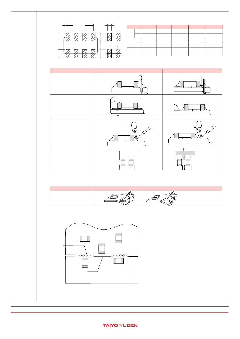
�Excess� solder� can� affect� the� ability� of� chips� to� withstand� mechanical� stresses.� Therefore,� please� take� proper� precautions� when�
�designing� land-patterns.�
�c�
�d�
�c�
�Recommended� land� dimension� for� Reflow-soldering�
�Type�
�3216�
�2010�
�1210�
�0806�
�0605�
�Size�
�L� 3.2� 2.0� 1.25� 0.85� 0.65�
�W� 1.6� 1.0� 1.0� 0.65� 0.50�
�a� 0.7~0.9� 0.5~0.6�
�0.45~0.55� 0.25~0.35� 0.27~0.33�
�d�
�b� 0.8~1.0�
�0.5~0.6�
�0.7~0.8�
�0.25~0.35� 0.17~0.23�
�((2)� Examples� of� good� and� bad� solder� application�
�c� 0.4~0.5�
�d� 0.8�
�(Unit:mm)�
�0.2~0.3�
�0.5�
�0.25~0.35� 0.25~0.35� 0.20~0.26�
�0.55� 0.5� 0.4�
�Item�
�Not� recommended�
�Lead� wire� of� component�
�Recommended�
�Solder-resist�
�Mixed� mounting� of� SMD� and�
�leaded� components�
�Chassis�
�Component� placement� close� to�
�the� chassis�
�Solder� (for� grounding)�
�Electrode� pattern�
�Lead� wire� of� component�
�Solder-resist�
�Hand-soldering� of� leaded�
�Soldering� iron�
�Solder-resist�
�components� near� mounted�
�components�
�Solder-resist�
�Horizontal� component�
�placement�
�◆Pattern� configurations(Inductor� layout� on� panelized[� breakaway]� PC� boards)�
�1-1.� The� following� are� examples� of� good� and� bad� inductor� layout;� SMD� inductors� should� be� located� to� minimize� any� possible� mechanical�
�stresses� from� board� warp� or� deflection.�
�Item�
�Deflection� of� the� board�
�Not� recommended�
�Recommended�
�Position� the� component� at� a�
�right� angle� to� the� direction� of�
�the� mechanical� stresses� that�
�are� anticipated.�
�1-2.� To� layout� the� inductors� for� the� breakaway� PC� board,� it� should� be� noted� that� the� amount� of� mechanical� stresses� given� will� vary�
�depending� on� inductor� layout.�
�An� example� below� should� be� counted� for� better� design.�
�E�
�D�
�Perforation�
�C�
�A�
�Slit�
�B�
�Magnitude� of� stress�
�A>B=C>D>E�
�1-3.� When� breaking� PC� boards� along� their� perforations,� the� amount� of� mechanical� stress� on� the� inductors� can� vary� according� to� the�
�method� used.� The� following� methods� are� listed� in� order� from� least� stressful� to� most� stressful:� push-back,� slit,� V-grooving,� and�
�perforation.� Thus,� any� ideal� SMD� inductor� layout� must� also� consider� the� PCB� splitting� procedure.�
�?� This� catalog� contains� the� typical� specification� only� due� to� the� limitation� of� space.� When� you� consider� the� purchase� of� our� products,� please� check� our� specification.�
�For� details� of� each� product� (characteristics� graph,� reliability� information,� precautions� for� use,� and� so� on),� see� our� Web� site� (http://www.ty-top.com/)� .�
�i_mlci_prec_e-E02R01�
�相关PDF资料 |
PDF描述 |
|---|---|
| BRL2518T2R2M | INDUCTOR 2.2UH 20% 1007 SMD |
| EBM12DSEN-S13 | CONN EDGECARD 24POS .156 EXTEND |
| R0.25S-0509/H-R | CONV DC/DC 0.25W 5V IN 9V OUT |
| LK16085R6K-T | INDUCTOR 5.6UH 10% 0603 SMD |
| EEU-FR1V680B | CAP ALUM 68UF 35V 20% RADIAL |
相关代理商/技术参数 |
参数描述 |
|---|---|
| LK1608100K-T | 制造商:TAIYO YUDEN 功能描述:Inductor Series:LF LK 制造商:TAIYO YUDEN 功能描述:MULTI-LAYER SMD INDUCTOR |
| LK-1608-100KTK | 功能描述:固定电感器 10uH 5mA 10% Wound Chip RoHS:否 制造商:AVX 电感:10 uH 容差:20 % 最大直流电流:1 A 最大直流电阻:0.075 Ohms 工作温度范围:- 40 C to + 85 C 自谐振频率:38 MHz Q 最小值:40 尺寸:4.45 mm W x 6.6 mm L x 2.92 mm H 屏蔽:Shielded 端接类型:SMD/SMT 封装 / 箱体:6.6 mm x 4.45 mm |
| LK1608100M-T | 功能描述:固定电感器 INDCTR STD MULTILYR 0603 10uH 20% RoHS:否 制造商:AVX 电感:10 uH 容差:20 % 最大直流电流:1 A 最大直流电阻:0.075 Ohms 工作温度范围:- 40 C to + 85 C 自谐振频率:38 MHz Q 最小值:40 尺寸:4.45 mm W x 6.6 mm L x 2.92 mm H 屏蔽:Shielded 端接类型:SMD/SMT 封装 / 箱体:6.6 mm x 4.45 mm |
| LK1608120K-T | 功能描述:固定电感器 INDCTR STD MULTILYR 0603 12uH 10% RoHS:否 制造商:AVX 电感:10 uH 容差:20 % 最大直流电流:1 A 最大直流电阻:0.075 Ohms 工作温度范围:- 40 C to + 85 C 自谐振频率:38 MHz Q 最小值:40 尺寸:4.45 mm W x 6.6 mm L x 2.92 mm H 屏蔽:Shielded 端接类型:SMD/SMT 封装 / 箱体:6.6 mm x 4.45 mm |
| LK-1608-120KTK | 功能描述:固定电感器 12uH 5mA 10% RoHS:否 制造商:AVX 电感:10 uH 容差:20 % 最大直流电流:1 A 最大直流电阻:0.075 Ohms 工作温度范围:- 40 C to + 85 C 自谐振频率:38 MHz Q 最小值:40 尺寸:4.45 mm W x 6.6 mm L x 2.92 mm H 屏蔽:Shielded 端接类型:SMD/SMT 封装 / 箱体:6.6 mm x 4.45 mm |
发布紧急采购,3分钟左右您将得到回复。