- 您现在的位置:买卖IC网 > PDF目录385474 > LM12L458 (National Semiconductor Corporation) 12-Bit Sign Data Acquisition System with Self-Calibration PDF资料下载
参数资料
| 型号: | LM12L458 |
| 厂商: | National Semiconductor Corporation |
| 英文描述: | 12-Bit Sign Data Acquisition System with Self-Calibration |
| 中文描述: | 12位注册数据采集系统自校准 |
| 文件页数: | 21/36页 |
| 文件大小: | 695K |
| 代理商: | LM12L458 |
第1页第2页第3页第4页第5页第6页第7页第8页第9页第10页第11页第12页第13页第14页第15页第16页第17页第18页第19页第20页当前第21页第22页第23页第24页第25页第26页第27页第28页第29页第30页第31页第32页第33页第34页第35页第36页
2.0 Internal User-Programmable Registers
(Continued)
Bits 12–15
are used to store the user-programmable acqui-
sition time. The Sequencer keeps the internal S/H in the ac-
quisition mode for a fixed number of clock cycles (nine clock
cycles, for 12-bit + sign conversions and two clock cycles for
8-bit + sign conversions or “watchdog” comparisons) plus a
variable number of clock cycles equal to twice the value
stored in Bits 12–15. Thus, the S/H’s acquisition time is (9 +
2D) clock cycles for 12-bit + sign conversions and (2 + 2D)
clock cycles for 8-bit + sign conversions or “watchdog” com-
parisons, where D is the value stored in Bits 12–15. The
minimum acquisition time compensates for the typical inter-
nal multiplexer series resistance of 2 k
, and any additional
delay created by Bits 12–15 compensates for source resis-
tances greater than 80
. (For this acquisition time discus-
sion, numbers in ( ) are shown for the LM12L458 operating
at 6 MHz. The necessary acquisition time is determined by
the source impedance at the multiplexer input. If the source
resistance (R
S
)
<
80
and the clock frequency is 6 MHz, the
value stored in bits 12–15 (D) can be 0000. If R
>
80
, the
following equations determine the value that should be
stored in bits 12–15.
D = 0.45 x R
S
x f
CLK
for 12-bits + sign
D = 0.36 x R
S
x f
CLK
for 8-bits + sign and “watchdog”
R
is in k
and f
is in MHz. Round the result to the next
higher integer value. If D is greater than 15, it is advisable to
lower the source impedance by using an analog buffer be-
tween the signal source and the LM12L458’s multiplexer in-
puts.
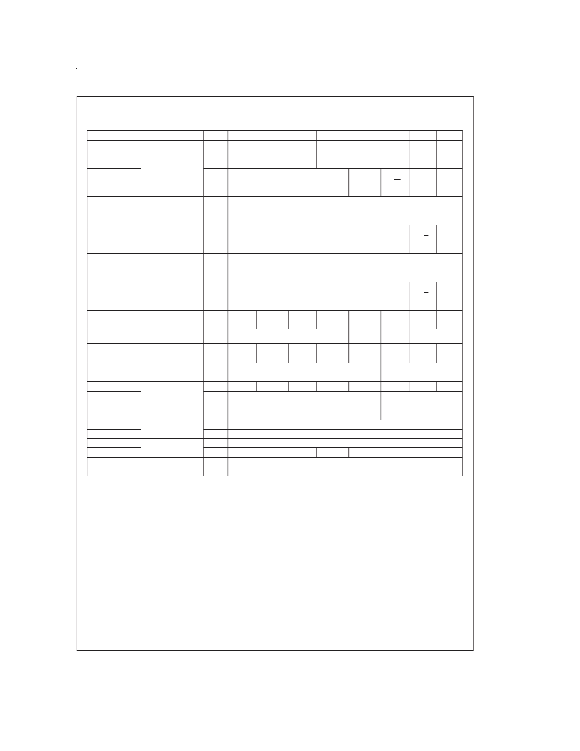
Instruction RAM “01”
The second Instruction RAM section is selected by placing a
“01” in Bits 8 and 9 of the Configuration register.
A4 A3 A2 A1 A0
0
0
to
1
0
0
to
1
0
0
to
1
0
0
to
1
0
0
to
1
0
0
to
1
1
0
Purpose
Type
D7
D6
D5
D4
D3
D2
D1
D0
0
0
(Instruction RAM
V
IN
V
IN+
0
R/W
Pause
Loop
1
0
1
0
Watch-
dog
1
R/W
Acquisition Time
8/12
Timer
Sync
1
0
1
0
(Instruction RAM
0
R/W
Comparison Limit
#
1
1
0
1
0
1
R/W
Don’t Care
>
/
<
Sign
1
0
1
0
(Instruction RAM
0
R/W
Comparison Limit
#
2
1
0
1
0
1
R/W
Don’t Care
>
/
<
Sign
1
0
1
0
0
Configuration
Register
R/W
I/O
Sel
Auto
Zero
ec
Chan
Mask
Stand-
by
Full
Cal
Auto-
Zero
Test
= 0
Reset
Start
1
0
0
0
1
R/W
Don’t Care
DIAG
RAM Pointer
1
0
0
1
0
Interrupt Enable
Register
R/W
INT7
Don’t
Care
INT5
INT4
INT3
INT2
INT1
INT0
1
0
0
1
1
R/W
Number of Conversions in Conversion
FIFO to Generate INT2
“0”
INST5
Sequencer Address to
Generate INT1
INST2
INST1
Address of Sequencer
Instruction
being Executed
1
1
0
0
1
1
0
0
0
1
Interrupt Status
Register
R
R
INST7
INST4
INST3
INST0
Actual Number of Conversions Results in Conversion
FIFO
1
1
1
1
1
1
0
0
1
1
1
1
1
1
0
0
0
0
1
1
0
0
1
1
0
1
0
1
0
1
Timer
Register
R/W
R/W
R
R
R
R
Timer Preset: Low Byte
Timer Preset: High Byte
Conversion Data: LSBs
Sign
Limit
#
1 Status
Limit
#
2 Status
Conversion
FIFO
Address or Sign
Conversion Data: MSBs
Limit Status
Register
FIGURE 14. LM12L458 Memory Map for 8-Bit Wide Databus (BW = “1” and Test Bit = “0”)
www.national.com
21
相关PDF资料 |
PDF描述 |
|---|---|
| LM133 | 3-Ampere Adjustable Negative Regulators |
| LM333T | 3-Ampere Adjustable Negative Regulators |
| LM133K | 3-Ampere Adjustable Negative Regulators |
| LM13600 | Dual Operational Transconductance Amplifiers with Linearizing Diodes and Buffers |
| LM13600AN | Dual Operational Transconductance Amplifiers with Linearizing Diodes and Buffers |
相关代理商/技术参数 |
参数描述 |
|---|---|
| LM12L458_06 | 制造商:NSC 制造商全称:National Semiconductor 功能描述:12-Bit + Sign Data Acquisition System with Self-Calibration |
| LM12L458CIV | 功能描述:模数转换器 - ADC RoHS:否 制造商:Texas Instruments 通道数量:2 结构:Sigma-Delta 转换速率:125 SPs to 8 KSPs 分辨率:24 bit 输入类型:Differential 信噪比:107 dB 接口类型:SPI 工作电源电压:1.7 V to 3.6 V, 2.7 V to 5.25 V 最大工作温度:+ 85 C 安装风格:SMD/SMT 封装 / 箱体:VQFN-32 |
| LM12L458CIV/NOPB | 功能描述:模数转换器 - ADC RoHS:否 制造商:Texas Instruments 通道数量:2 结构:Sigma-Delta 转换速率:125 SPs to 8 KSPs 分辨率:24 bit 输入类型:Differential 信噪比:107 dB 接口类型:SPI 工作电源电压:1.7 V to 3.6 V, 2.7 V to 5.25 V 最大工作温度:+ 85 C 安装风格:SMD/SMT 封装 / 箱体:VQFN-32 |
| LM12L458CIVF | 制造商:Rochester Electronics LLC 功能描述:12-BIT PARALLEL I/O DAS - Bulk |
| LM12L458CIVF/NOPB | 制造商:Texas Instruments 功能描述:ADC Single 114ksps 12-bit+Sign Parallel 44-Pin PLCC |
发布紧急采购,3分钟左右您将得到回复。