- 您现在的位置:买卖IC网 > PDF目录30743 > LM1596H/883 (NATIONAL SEMICONDUCTOR CORP) SPECIALTY CONSUMER CIRCUIT, MBCY10 PDF资料下载
参数资料
| 型号: | LM1596H/883 |
| 厂商: | NATIONAL SEMICONDUCTOR CORP |
| 元件分类: | 消费家电 |
| 英文描述: | SPECIALTY CONSUMER CIRCUIT, MBCY10 |
| 封装: | METAL CAN, 10 PIN |
| 文件页数: | 2/4页 |
| 文件大小: | 163K |
| 代理商: | LM1596H/883 |
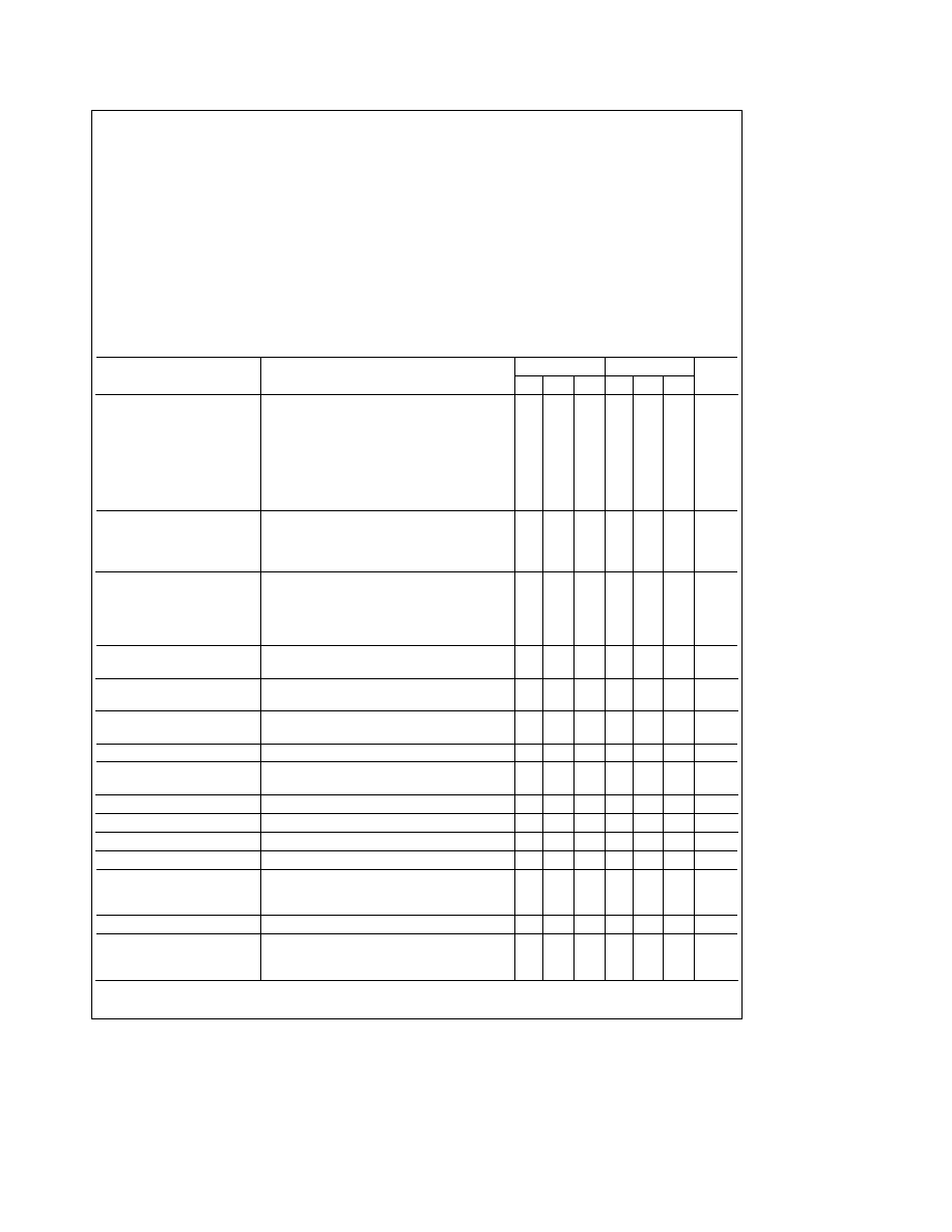
Absolute Maximum Ratings
If MilitaryAerospace specified devices are required
please contact the National Semiconductor Sales
OfficeDistributors for availability and specifications
Internal Power Dissipation (Note 1)
500 mW
Applied Voltage (Note 2)
30V
Differential Input Signal (V7 b V8)
g
50V
Differential Input Signal (V4 b V1)
g
(5aI5R0)V
Input Signal (V2 b V1 V3 b V4)
50V
Bias Current (I5)12 mA
Operating Temperature Range LM1596 b55 Cto a125 C
LM1496
0 Cto a70 C
Storage Temperature Range
b
65 Cto a150 C
Soldering Information
Dual-In-Line Package
Soldering (10 seconds)
260 C
Small Outline Package
Vapor Phase (60 seconds)
215 C
Infrared (15 seconds)
220 C
See AN-450 ‘‘Surface Mounting Methods and their effects
on Product Reliability’’ for other methods of soldering sur-
face mount devices
Electrical Characteristics (TA e 25 C unless otherwise specified see test circuit)
Parameter
Conditions
LM1596
LM1496
Units
Min
Typ
Max Min
Typ
Max
Carrier Feedthrough
VC e 60 mVrms sine wave
40
m
Vrms
fC e 10 kHz offset adjusted
VC e 60 mVrms sine wave
140
m
Vrms
fC e 10 kHz offset adjusted
VC e 300 mVpp square wave
004
02
004
02
mVrms
fC e 10 kHz offset adjusted
VC e 300 mVpp square wave
20
100
20
150
mVrms
fC e 10 kHz not offset adjusted
Carrier Suppression
fS e 10 kHz 300 mVrms
50
65
50
65
dB
fC e 500 kHz 60 mVrms sine wave offset adjusted
fS e 10 kHz 300 mVrms
50
dB
fC e 10 MHz 60 mVrms sine wave offset adjusted
Transadmittance Bandwidth
RL e 50X
300
MHz
Carrier Input Port VC e 60 mVrms sine wave
fS e 10 kHz 300 mVrms sine wave
Signal Input Port VS e 300 mVrms sine wave
80
MHz
V7 b V8 e 05Vdc
Voltage Gain Signal Channel
VS e 100 mVrms fe 10 kHz
25
35
25
35
VV
V7 b V8 e 05 Vdc
Input Resistance Signal Port
f e 50 MHz
200
kX
V7 b V8 e 05 Vdc
Input Capacitance Signal Port
f e 50 MHz
20
pF
V7 b V8 e 05 Vdc
Single Ended Output Resistance f e 10 MHz
40
kX
Single Ended Output
f e 10 MHz
50
pF
Capacitance
Input Bias Current
(I1 a I4)2
12
25
12
30
m
A
Input Bias Current
(I7 a I8)2
12
25
12
30
m
A
Input Offset Current
(I1 b I4)
07
50
07
50
m
A
Input Offset Current
(I7 b I8)
07
50
m
A
Average Temperature
(b55 C k TA k a125 C)
20
nA C
Coefficient of Input
(0 C k TA k a70 C)
20
nA C
Offset Current
Output Offset Current
(I6 b I9)
1450
1460
m
A
Average Temperature
(b55 C k TA k a125 C)
90
nA C
Coefficient of Output
(0 C k TA k a70 C)
90
nA C
Offset Current
2
相关PDF资料 |
PDF描述 |
|---|---|
| LM1596H-MIL | SPECIALTY CONSUMER CIRCUIT, MBCY10 |
| LM1812N | SPECIALTY CONSUMER CIRCUIT, PDIP18 |
| LM1837N | 2 CHANNEL, AUDIO PREAMPLIFIER, PDIP18 |
| LM1837M | 2 CHANNEL, AUDIO PREAMPLIFIER, PDSO16 |
| LM1851N | POWER SUPPLY SUPPORT CKT, PDIP8 |
相关代理商/技术参数 |
参数描述 |
|---|---|
| LM159-70 2-135 | 制造商:MISCELLANEOUS 功能描述: |
| LM15X11 | 制造商:SHARP 制造商全称:Sharp Electrionic Components 功能描述:Color STN-LCD Module |
| LM15X80 | 制造商:SHARP 制造商全称:Sharp Electrionic Components 功能描述:Color STN-LCD Module(Desktop PC/Monitor) |
| LM-16 | 制造商:Mac8 功能描述:LEDpXy[T[ - KLEDaF3/ 5AKLEDsb`F-AtF - 125 -40 |
| LM160 | 制造商:Pulse 功能描述:- Bulk |
发布紧急采购,3分钟左右您将得到回复。