- 您现在的位置:买卖IC网 > PDF目录30743 > LM1837M (NATIONAL SEMICONDUCTOR CORP) 2 CHANNEL, AUDIO PREAMPLIFIER, PDSO16 PDF资料下载
参数资料
| 型号: | LM1837M |
| 厂商: | NATIONAL SEMICONDUCTOR CORP |
| 元件分类: | 音频/视频放大 |
| 英文描述: | 2 CHANNEL, AUDIO PREAMPLIFIER, PDSO16 |
| 封装: | DIP-16 |
| 文件页数: | 14/14页 |
| 文件大小: | 450K |
| 代理商: | LM1837M |
Application Hints (Continued)
TLH7902 – 14
TLH7902 – 15
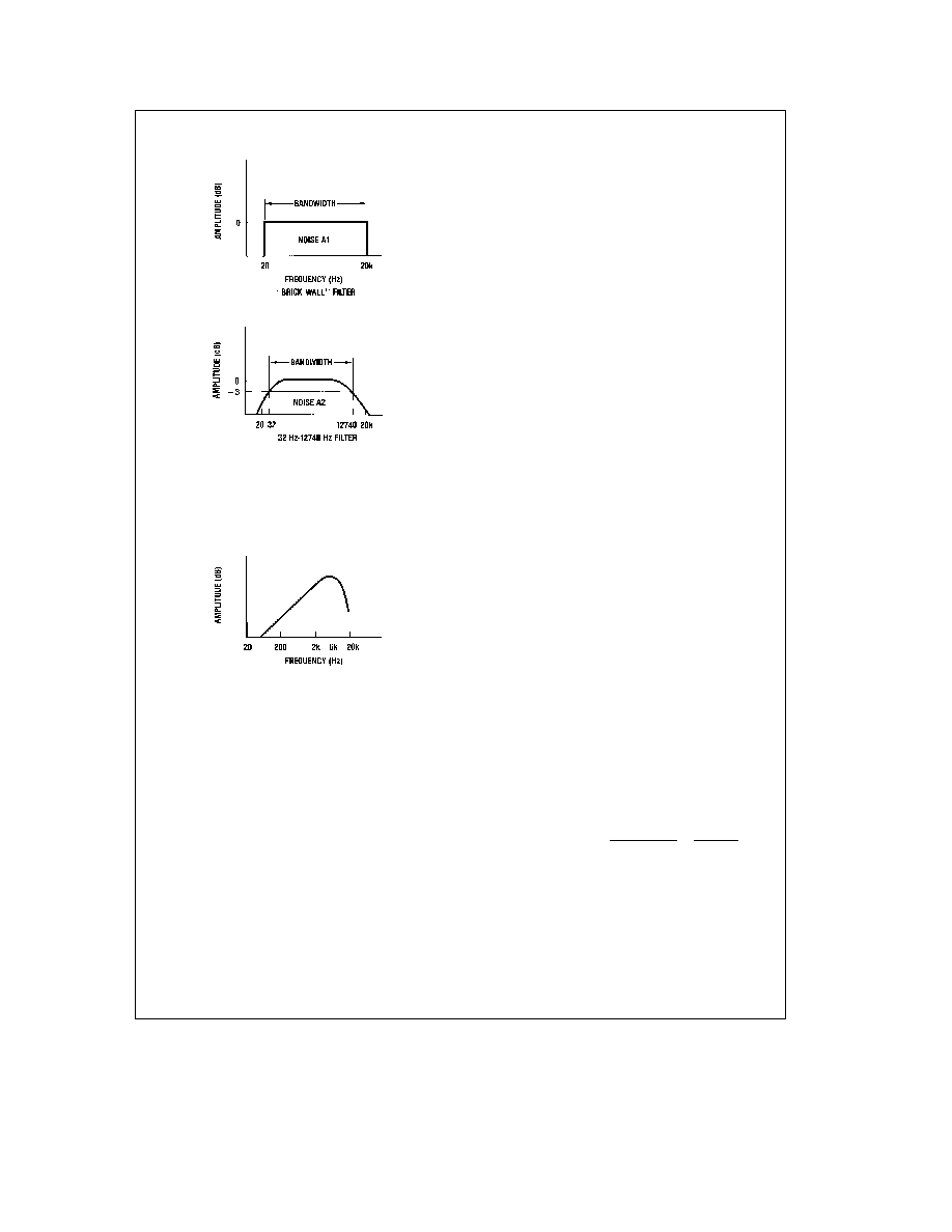
FIGURE 6
Typical signal-to-noise figures are listed for several weight-
ing filters which are commonly used in the measurement of
noise The shape of all weighting filters is similar with the
peak of the curve usually occurring in the 3 kHz – 7 kHz re-
gion as shown in
Figure 7
TLH7902 – 16
FIGURE 7
In addition to noise filtering differing meter types give differ-
ent noise readings Meter responses include 1) rms read-
ing 2) average responding 3) peak reading and 4) quasi
peak reading Although theoretical noise analysis is derived
using true rms (root mean square) based calculations most
actual measurement is taken with ARM (Average Respond-
ing Meter) test equipment
Unless otherwise noted an average responding meter is
used for all AC measurements in this data sheet
BASIC CIRCUIT APPROACH
The LM1837 IC incorporates a two stage broadband design
which minimizes noise attains overall DC stability and pre-
vents audible transients during turn-on
The first stage consists of four direct coupled preamplifiers
with internal gain of 25VV (28 dB) Direct coupling to the
tape head reduces input source impedance and external
component cost by removing the input coupling capacitor A
typical input coupling capacitor of 1 mF has a reactance of
15 kX at 100 Hz The resulting noise due to the amplifier’s
input noise current can dominate the noise voltage at the
output of the playback system The inputs of the amplifiers
are biased from a common reference voltage that is temper-
ature compensated to produce a quiescent DC voltage of
25V at the output of the first stage The input stage bias
current that flows through the tape head is kept below 2 mA
in order to prevent any erasure of tape moving past the
head An added advantage of DC biasing is the prevention
of large current transients during the charging of coupling
capacitors at turn-on and turn-off The outputs of the for-
ward and reverse preamplifier are fed to the common output
op amp through a logic controlled switch
The second stage provides additional gain and proper
equalization while preventing audible turn-on transients or
‘‘pops’’ The output (pin 2) is kept low until C2 charges
through R1 When the voltage on C2 gets close to the DC
voltage on pin 5 the output rises exponentially to its final
DC value The result is a transient-free turn-on characteris-
tic
Internal diodes are provided to facilitate electronic diode
switching popular in automotive applications
The General Test Circuit illustrates the topography of the
system The components determining the overall frequency
response are external due to the extreme sensitivity when
matching a DIN equalization curve
MUTE CIRCUIT AND LOGIC
The LM1837 can be muted with the addition of two resistors
and a grounding switch as shown in
Figure 1 When the
circuit is not muted the additional resistors have no effect on
the AC performance They
do have an effect on the DC Q
point however
The difference in the DC output voltages of the input amplifi-
ers is applied across the mute resistors (R7) and the posi-
tive input resistors (R1) This results in an additional offset
at the input of the output amplifiers To keep this offset to a
minimum R7 should be as large as possible to achieve ef-
fective muting Unmute voltage is the peak signal the pre-
amplifier can swing without turning on the output amplifier
under mute conditions
Unmute
voltage
e
VPIN 5 14
R5
UR3
R2 a R5
UR3
b
R7
R1 a R7
(
9
Obsolete
相关PDF资料 |
PDF描述 |
|---|---|
| LM1851N | POWER SUPPLY SUPPORT CKT, PDIP8 |
| LM1851M | POWER SUPPLY SUPPORT CKT, PDSO8 |
| LM1865MX | FM, AUDIO DEMODULATOR, PDSO20 |
| LM1875DWF | 25 W, 1 CHANNEL, AUDIO AMPLIFIER, UUC |
| LM1875LB02 | 25 W, 1 CHANNEL, AUDIO AMPLIFIER, PZFM5 |
相关代理商/技术参数 |
参数描述 |
|---|---|
| LM1837N | 制造商:NSC 制造商全称:National Semiconductor 功能描述:Low Noise PREAMPLIFIER FOR AUTOREVERSING TAPE PLAYBACK SYSTEMS |
| LM1837N/A+ | 制造商:未知厂家 制造商全称:未知厂家 功能描述:Preamp/Equalizer for Audio Tape Recorder |
| LM1837N/B+ | 制造商:未知厂家 制造商全称:未知厂家 功能描述:Preamp/Equalizer for Audio Tape Recorder |
| LM185 | 制造商:Texas Instruments 功能描述: |
| LM185_08 | 制造商:NSC 制造商全称:National Semiconductor 功能描述:Adjustable Micropower Voltage References |
发布紧急采购,3分钟左右您将得到回复。