- 您现在的位置:买卖IC网 > PDF目录30744 > LM1882E/883 (NATIONAL SEMICONDUCTOR CORP) SPECIALTY CONSUMER CIRCUIT, CQCC20 PDF资料下载
参数资料
| 型号: | LM1882E/883 |
| 厂商: | NATIONAL SEMICONDUCTOR CORP |
| 元件分类: | 消费家电 |
| 英文描述: | SPECIALTY CONSUMER CIRCUIT, CQCC20 |
| 封装: | CERAMIC, LCC-20 |
| 文件页数: | 14/16页 |
| 文件大小: | 236K |
| 代理商: | LM1882E/883 |
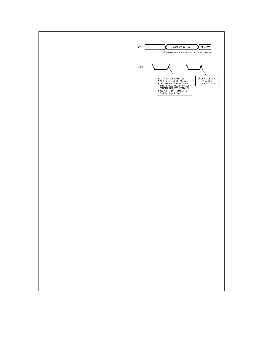
Addressing Logic (Continued)
ADDRDEC LOGIC
The ADDRDEC logic decodes the current address and gen-
erates the enable signal for the appropriate register The
enable values for the registers and counters change on the
falling edge of LOAD Two types of ADDRDEC logic is en-
abled by 2 pair of addresses Addresses 22 or 54 (Vectored
Restart logic) and Addresses 23 or 55 (Vectored Clear log-
ic) Loading these addresses will enable the appropriate log-
ic and put the part into either a Restart (all counter registers
are reinitialized with preprogrammed data) or Clear (all reg-
isters are cleared to zero) state
Reloading the same
ADDRDEC address will not cause any change in the state of
the part The outputs during these states are frozen and the
internal CLOCK is disabled Clocking the part during a Vec-
tored Restart or Vectored Clear state will have no effect on
the part To resume operation in the new state or disable
the Vectored Restart or Vectored Clear state another non-
ADDRDEC address must be loaded Operation will begin in
the new state on the rising edge of the non-ADDRDEC load
pulse It is recommended that an unused address be loaded
following an ADDRDEC operation to prevent data registers
from accidentally being corrupted The following Addresses
are used by the device
Address 0
Status Register REG0
Address 1 – 18
Data Registers REG1 – REG18
Address 19 – 21 Unused
Address 2254 Restart Vector (Restarts Device)
Address 2355 Clear Vector (Zeros All Registers)
Address 24 – 31 Unused
Address 32 – 50 Register Scan Addresses
Address 51 – 53 Counter Scan Addresses
Address 56 – 63 Unused
At any given time only one register at most is selected It is
possible to have no registers selected
VECTORED RESTART ADDRESS
The function of addresses 22 (16H) or 54 (36H) are similar
to that of the CLR pin except that the preprogramming of
the registers is not affected It is recommended but not re-
quired that this address is read after the initial device config-
uration load sequence A1onthe ADDRDATA pin (Auto
Addressing Mode) will not cause this address to automati-
cally increment The address will loop back onto itself re-
gardless of the state of ADDRDATA unless the address on
the Data inputs has been changed with ADDRDATA at 0
VECTORED CLEAR ADDRESS
Addresses 23 (17H) or 55 (37H) is used to clear all registers
to zero simultaneously This function may be desirable to
use prior to loading new data into the Data or Status Regis-
ters This address is read into the device in a similar fashion
as all of the other registers A1onthe ADDRDATA pin
(Auto Addressing Mode) will not cause this address to auto-
matically increment The address will loop back onto itself
regardless of the state of ADDRDATA unless the address
on the Data inputs has been changed with ADDRDATA at 0
TLF10137 – 9
FIGURE 3 ADDRDEC Timing
GEN LOCKING
The ’ACT715LM1882 and ’ACT715-RLM1882-R is de-
signed for master SYNC and BLANK signal generation
However the devices can be synchronized (slaved) to an
external timing signal in a limited sense Using Vectored
Restart the user can reset the counting sequence to a giv-
en location the beginning at a given time the rising edge of
the LOAD that removes Vector Restart At this time the next
CLOCK pulse will be CLOCK 1 and the count will restart at
the beginning of the first odd line
Preconditioning the part during normal operation before the
desired synchronizing pulse is necesasry However since
LOAD and CLOCK are asynchronous and independent this
is possible without interruption or data and performance cor-
ruption If the defaulted 1431818 MHz RS-170 values are
being used preconditioning and restarting can be minimized
by using the CLEAR pulse instead of the Vectored Restart
operation The ’ACT715-RLM1882-R is better suited for
this application because it eliminates the need to program a
1 into Bit 10 of the Status Register to enable the CLOCK
Gen Locking to another count location other than the very
beginning or separate horizontalvertical resetting is not
possible with the ’ACT715LM1882 nor the ’ACT715-R
LM1882-R
SCAN MODE LOGIC
A scan mode is available in the ACT715LM1882 that al-
lows the user to non-destructively verify the contents of the
registers Scan mode is invoked through reading a scan ad-
dress into the address register The scan address of a given
register is defined by the Data register address a 32 The
internal Clocking signal is disabled when a scan address is
read Disabling the clock freezes the device in it’s present
state Data can then be serially scanned out of the data
registers through the ODDEVEN Pin The LSB will be
scanned out first Since each register is 12 bits wide com-
pletely scanning out data of the addressed register will re-
quire 12 CLOCK pulses More than 12 CLOCK pulses on the
same register will only cause the MSB to repeat on the out-
put Re-scanning the same register will require that register
to be reloaded The value of the two horizontal counters and
1 vertical counter can also be scanned out by using address
numbers 51 – 53 Note that before the part will scan out the
data the LOAD signal must be brought back HIGH
7
相关PDF资料 |
PDF描述 |
|---|---|
| LM1882J/883 | SPECIALTY CONSUMER CIRCUIT, CDIP20 |
| LM1882RE/883 | SPECIALTY CONSUMER CIRCUIT, CQCC20 |
| LM1882RJ/883 | SPECIALTY CONSUMER CIRCUIT, CDIP20 |
| LM1882EV | SPECIALTY CONSUMER CIRCUIT, PQCC20 |
| LM1882-REV | SPECIALTY CONSUMER CIRCUIT, CQCC20 |
相关代理商/技术参数 |
参数描述 |
|---|---|
| LM1882-R | 制造商:NSC 制造商全称:National Semiconductor 功能描述:Programmable Video Sync Generator |
| LM1882RCM | 制造商:未知厂家 制造商全称:未知厂家 功能描述:TV/Video Sync Circuit |
| LM1882-RCM | 制造商:NSC 制造商全称:National Semiconductor 功能描述:Programmable Video Sync Generator |
| LM1882RCN | 制造商:未知厂家 制造商全称:未知厂家 功能描述:TV/Video Sync Circuit |
| LM1882-RCN | 制造商:NSC 制造商全称:National Semiconductor 功能描述:Programmable Video Sync Generator |
发布紧急采购,3分钟左右您将得到回复。