- 您现在的位置:买卖IC网 > PDF目录30744 > LM1882J/883 (NATIONAL SEMICONDUCTOR CORP) SPECIALTY CONSUMER CIRCUIT, CDIP20 PDF资料下载
参数资料
| 型号: | LM1882J/883 |
| 厂商: | NATIONAL SEMICONDUCTOR CORP |
| 元件分类: | 消费家电 |
| 英文描述: | SPECIALTY CONSUMER CIRCUIT, CDIP20 |
| 封装: | CERAMIC, DIP-20 |
| 文件页数: | 9/16页 |
| 文件大小: | 236K |
| 代理商: | LM1882J/883 |
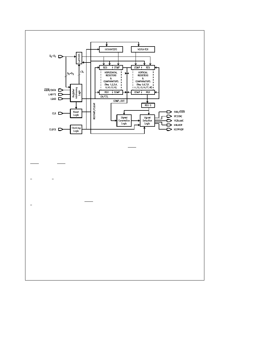
Logic Block Diagram
TLF10137 – 3
Pin Description
There are a Total of 13 inputs and 5 outputs on the
’ACT715LM1882
Data Inputs D0 – D7
The Data Input pins connect to the
Address Register and the Data Input Register
ADDR DATA
The ADDR DATA signal is latched into the
device on the falling edge of the LOAD signal The signal
determines if an address (0) or data (1) is present on the
data bus
L HBYTE
The L HBYTE signal is latched into the device
on the falling edge of the LOAD signal The signal deter-
mines if data will be read into the 8 LSB’s (0) or the 4 MSB’s
(1) of the Data Registers A1on this pin when an ADDR
DATA is a 0 enables Auto-Load Mode
LOAD
The LOAD control pin loads data into the Address or
Data Registers on the rising edge
ADDR DATA and
L HBYTE data is loaded into the device on the falling edge
of the LOAD The LOAD pin has been implemented as a
Schmitt trigger input for better noise immunity
CLOCK
System CLOCK input from which all timing is de-
rived The clock pin has been implemented as a Schmitt
trigger for better noise immunity The CLOCK and the LOAD
signal are asynchronous and independent Output state
changes occur on the falling edge of CLOCK
CLR
The CLEAR pin is an asynchronous input that initializ-
es the device when it is HIGH Initialization consists of set-
ting all registers to their mask programmed values and ini-
tializing all counters
comparators and registers
The
CLEAR pin has been implemented as a Schmitt trigger for
better noise immunity A CLEAR pulse should be asserted
by the user immediately after power-up to ensure proper
initialization of the registerseven if the user plans to
(re)program the device
Note
A CLEAR pulse will disable the CLOCK on the ’ACT715LM1882 and
will enable the CLOCK on the ’ACT715-RLM1882-R
ODDEVEN
Output that identifies if display is in odd (HIGH)
or even (LOW) field of interlace when device is in interlaced
mode of operation In noninterlaced mode of operation this
output is always HIGH Data can be serially scanned out on
this pin during Scan Mode
VCSYNC
Outputs Vertical or Composite Sync signal based
on value of the Status Register Equalization and Serration
pulses will (if enabled) be output on the VCSYNC signal in
composite mode only
VCBLANK
Outputs Vertical or Composite Blanking signal
based on value of the Status Register
HBLHDR
Outputs Horizontal Blanking signal Horizontal
Gating signal or Cursor Position based on value of the
Status Register
HSYNVDR
Outputs Horizontal Sync signal Vertical Gating
signal or Vertical Interrupt signal based on value of Status
Register
Register Description
All of the data registers are 12 bits wide Width’s of all puls-
es are defined by specifying the start count and end count
of all pulses Horizontal pulses are specified with-respect-to
the number of clock pulses per line and vertical pulses are
specified with-respect-to the number of lines per frame
REG0STATUS REGISTER
The Status Register controls the mode of operation the
signals that are output and the polarity of these outputs The
default value for the Status Register is 0 (000 Hex) for the
’ACT715LM1882 and is ‘‘512’’ (200 Hex) for the ’ACT715-
RLM1882-R
2
相关PDF资料 |
PDF描述 |
|---|---|
| LM1882RE/883 | SPECIALTY CONSUMER CIRCUIT, CQCC20 |
| LM1882RJ/883 | SPECIALTY CONSUMER CIRCUIT, CDIP20 |
| LM1882EV | SPECIALTY CONSUMER CIRCUIT, PQCC20 |
| LM1882-REV | SPECIALTY CONSUMER CIRCUIT, CQCC20 |
| LM1894M/NOPB | SPECIALTY CONSUMER CIRCUIT, PDSO14 |
相关代理商/技术参数 |
参数描述 |
|---|---|
| LM1882-R | 制造商:NSC 制造商全称:National Semiconductor 功能描述:Programmable Video Sync Generator |
| LM1882RCM | 制造商:未知厂家 制造商全称:未知厂家 功能描述:TV/Video Sync Circuit |
| LM1882-RCM | 制造商:NSC 制造商全称:National Semiconductor 功能描述:Programmable Video Sync Generator |
| LM1882RCN | 制造商:未知厂家 制造商全称:未知厂家 功能描述:TV/Video Sync Circuit |
| LM1882-RCN | 制造商:NSC 制造商全称:National Semiconductor 功能描述:Programmable Video Sync Generator |
发布紧急采购,3分钟左右您将得到回复。