- 您现在的位置:买卖IC网 > PDF目录30744 > LM1894M/NOPB (NATIONAL SEMICONDUCTOR CORP) SPECIALTY CONSUMER CIRCUIT, PDSO14 PDF资料下载
参数资料
| 型号: | LM1894M/NOPB |
| 厂商: | NATIONAL SEMICONDUCTOR CORP |
| 元件分类: | 消费家电 |
| 英文描述: | SPECIALTY CONSUMER CIRCUIT, PDSO14 |
| 封装: | LEAD FREE, SOP-14 |
| 文件页数: | 5/12页 |
| 文件大小: | 340K |
| 代理商: | LM1894M/NOPB |
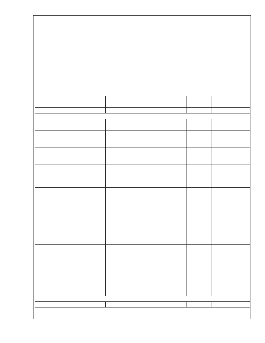
Absolute Maximum Ratings (Note 1)
If Military/Aerospace specified devices are required,
please contact the National Semiconductor Sales Office/
Distributors for availability and specifications.
Supply Voltage
20V
Input Voltage Range, V
pk
V
S/2
Operating Temperature (Note 2)
0C to +70C
Storage Temperature
65C to +150C
Soldering Information
Dual-In-Line Package
Soldering (10 seconds)
260C
Small Outline Package
Vapor Phase (60 seconds)
215C
Infrared (15 seconds)
220C
See AN-450 “Surface Mounting Methods and Their Effect
on Product Reliability” for other methods of soldering
surface mount devices.
Note 1: “Absolute Maximum Ratings” indicate limits beyond which damage
to the device may occur. Operating Ratings indicate conditions for which the
device is functional, but do not guarantee specific performance limits.
Electrical Characteristics
V
Parameter
Conditions
Min
Typ
Max
Units
Operating Supply Range
4.5
8
18
V
Supply Current
V
S =8V
17
30
mA
MAIN SIGNAL PATH
Voltage Gain
DC Ground Pin 9, (Note 3)
0.9
1
1.1
V/V
DC Output Voltage
3.7
4.0
4.3
V
Channel Balance
DC Ground Pin 9
1.0
dB
Minimum Balance
AC Ground Pin 9 with 0.1 F
675
965
1400
Hz
Capacitor, (Note 3)
Maximum Bandwidth
DC Ground Pin 9, (Note 3)
27
34
46
kHz
Effective Noise Reduction
CCIR/ARM Weighted, (Note 4)
10
14
dB
Total Harmonic Distortion
DC Ground Pin 9
0.05
0.1
%
Input Headroom
Maximum V
IN for 3% THD
1.0
Vrms
AC Ground Pin 9
Output Headroom
Maximum V
OUT for 3% THD
V
S 1.5
Vp-p
DC Ground Pin 9
Signal to Noise
BW = 20 Hz–20 kHz, re 300 mV
AC Ground Pin 9
79
dB
DC Ground Pin 9
77
dB
CCIR/ARM Weighted re 300 mV
AC Ground Pin 9
82
88
dB
DC Ground Pin 9
70
76
dB
CCIR Peak, re 300 mV, (Note 6)
AC Ground Pin 9
77
dB
DC Ground Pin 9
64
dB
Input Impedance
Pin 2 and Pin 13
14
20
26
k
Channel Separation
DC Ground Pin 9
50
70
dB
Power Supply Rejection
C14 = 100 F,
V
RIPPLE = 500 mVrms,
40
56
dB
f=1kHz
Output DC Shift
Reference DVM to Pin 14 and
Measuree Output DC Shift from
4.0
20
mV
Minimum to Maximum Band-
width, (Note 7).
CONTROL SIGNAL PATH
Summing Amplifier Voltage Gain
Both Channels Driven
0.9
1
1.1
V/V
LM1894
www.national.com
2
相关PDF资料 |
PDF描述 |
|---|---|
| LM1894MDC | SPECIALTY CONSUMER CIRCUIT, UUC |
| LM1894MWC | SPECIALTY CONSUMER CIRCUIT, UUC |
| LM1894MT/NOPB | SPECIALTY CONSUMER CIRCUIT, PDSO14 |
| LM1894MTX/NOPB | SPECIALTY CONSUMER CIRCUIT, PDSO14 |
| LM1897N | 2 CHANNEL, AUDIO AMPLIFIER, PDIP16 |
相关代理商/技术参数 |
参数描述 |
|---|---|
| LM1894MT | 制造商:未知厂家 制造商全称:未知厂家 功能描述: |
| LM1894MTBD | 功能描述:BOARD EVALUATION LM1894 RoHS:否 类别:编程器,开发系统 >> 评估演示板和套件 系列:- 标准包装:1 系列:PCI Express® (PCIe) 主要目的:接口,收发器,PCI Express 嵌入式:- 已用 IC / 零件:DS80PCI800 主要属性:- 次要属性:- 已供物品:板 |
| LM1894MX | 功能描述:特殊用途放大器 RoHS:否 制造商:Texas Instruments 通道数量:Single 共模抑制比(最小值): 输入补偿电压: 工作电源电压:3 V to 5.5 V 电源电流:5 mA 最大功率耗散: 最大工作温度:+ 70 C 最小工作温度:- 40 C 安装风格:SMD/SMT 封装 / 箱体:QFN-20 封装:Reel |
| LM1894MX/NOPB | 功能描述:特殊用途放大器 RoHS:否 制造商:Texas Instruments 通道数量:Single 共模抑制比(最小值): 输入补偿电压: 工作电源电压:3 V to 5.5 V 电源电流:5 mA 最大功率耗散: 最大工作温度:+ 70 C 最小工作温度:- 40 C 安装风格:SMD/SMT 封装 / 箱体:QFN-20 封装:Reel |
| LM1894N | 制造商:Rochester Electronics LLC 功能描述:- Bulk 制造商:OC White Company 功能描述:Dynamic Noise Reduction System 14-Pin PDIP Rail |
发布紧急采购,3分钟左右您将得到回复。