- 您现在的位置:买卖IC网 > PDF目录30744 > LM1971MWC (NATIONAL SEMICONDUCTOR CORP) SPECIALTY CONSUMER CIRCUIT, UUC PDF资料下载
参数资料
| 型号: | LM1971MWC |
| 厂商: | NATIONAL SEMICONDUCTOR CORP |
| 元件分类: | 消费家电 |
| 英文描述: | SPECIALTY CONSUMER CIRCUIT, UUC |
| 封装: | WAFER |
| 文件页数: | 11/13页 |
| 文件大小: | 290K |
| 代理商: | LM1971MWC |
Application Information (Continued)
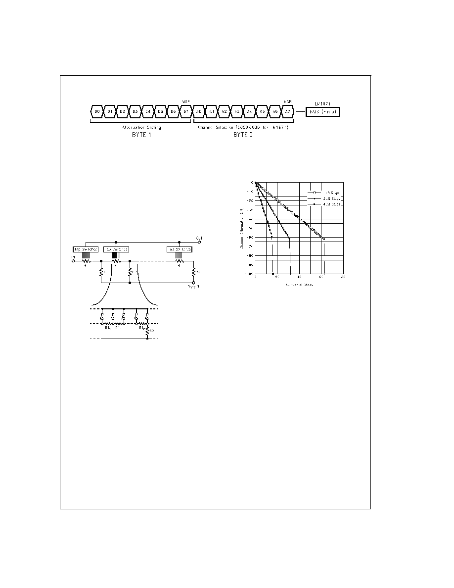
POT LADDER ARCHITECTURE
The Pot contains a chain of R1/R2 resistor dividers in a lad-
der form, as shown in
Figure 4. Each R1 is actually a series
of 8 resistors, with a CMOS switch that taps into the resistor
chain according to the attenuation level chosen. For any
given attenuation setting, there is only one CMOS switch
closed (no paralleling of ladders). The input impedance
therefore remains constant, while the output impedance
changes as the attenuation level changes. It is important to
note that the architecture is a series of resistor dividers, and
not a straight, tapped resistor, so the Pot is not a variable
resistor; it is a variable voltage divider.
ATTENUATION STEP SCHEME
The fundamental attenuation step scheme for the LM1971 is
shown in
Figure 5. It is also possible to obtain any integer
value attenuation step through programming, in addition to
the 2 dB and 4 dB steps shown in
Figure 5. All higher attenu-
ation step schemes can have clickless and popless perfor-
mance. Although it is possible to “skip” attenuation points by
not sending all of the data, clickless and popless perfor-
mance will suffer. It is highly recommended that all of the
data points should be sent for each attenuation level. This
ensures flawless operation and performance when making
steps larger than 1 dB.
INPUT IMPEDANCE
The input impedance of a Pot is constant at a nominal
40 k
. Since the LM1971 is a single-supply operating de-
vice, it is necessary to have both input and output coupling
caps as shown in
Figure 1. To ensure full low-frequency re-
sponse,a1F coupling cap should be used.
OUTPUT IMPEDANCE
The output impedance of a Pot varies typically between
25 k
and 35 k and changes nonlinearly with step
changes. Since a Pot is made up of a resistor ladder net-
work with logarithmic attenuation, the output impedance is
nonlinear. Due to this configuration, a Pot cannot be con-
sidered as a linear potentiometer; it is a logarithmic attenua-
tor.
The linearity of a Pot cannot be measured directly without a
buffer because the input impedance of most measurement
systems is not high enough to provide the required accuracy.
The lower impedance of the measurement system would
load down the output and an incorrect reading would result.
To prevent loading, a JFET input op amp should be used as
the buffer/amplifier.
OUTPUT BUFFERING
There are two performance issues to be aware of that are re-
lated to a Pot’s output stage. The first concern is to prevent
audible clicks with attenuation changes, while the second is
to prevent loading and subsequent linearity errors. The out-
put stage of a Pot needs to be buffered with a low input bias
DS012353-4
FIGURE 3. Serial Data Format Transfer Process
DS012353-5
FIGURE 4. Resistor Ladder Architecture
LM 1971 Channel Attenuation
vs Digital Step Value
(1 dB, 2 dB, and 4 dB Steps)
DS012353-6
FIGURE 5. LM1971 Attenuation Step Scheme
www.national.com
7
相关PDF资料 |
PDF描述 |
|---|---|
| LM1972MNOPB | SPECIALTY CONSUMER CIRCUIT, PDSO20 |
| LM1972NNOPB | SPECIALTY CONSUMER CIRCUIT, PDIP20 |
| LM1972N/NOPB | SPECIALTY CONSUMER CIRCUIT, PDIP20 |
| LM1973N/NOPB | SPECIALTY CONSUMER CIRCUIT, PDIP20 |
| LM2005T | 11 W, 2 CHANNEL, AUDIO AMPLIFIER, PSFM11 |
相关代理商/技术参数 |
参数描述 |
|---|---|
| LM1971MX | 功能描述:衰减器 -IC RoHS:否 制造商:Skyworks Solutions, Inc. 最大衰减:18 dB 容差: 阻抗: 功率额定值:30 dBm 安装风格:SMD/SMT 工作温度范围:- 40 C to + 85 C |
| LM1971MX/NOPB | 功能描述:衰减器 -IC RoHS:否 制造商:Skyworks Solutions, Inc. 最大衰减:18 dB 容差: 阻抗: 功率额定值:30 dBm 安装风格:SMD/SMT 工作温度范围:- 40 C to + 85 C |
| LM1971N | 制造商:NSC 制造商全称:National Semiconductor 功能描述:LM1971 Overture⑩ Audio Attenuator Series Digitally Controlled 62 dB Audio Attenuator with/Mute |
| LM1971N/NOPB | 功能描述:IC ATTENUATOR AUDIO W/MUTE 8-DIP RoHS:是 类别:集成电路 (IC) >> 线性 - 音频处理 系列:Overture™ 其它有关文件:STA321 View All Specifications 标准包装:1 系列:Sound Terminal™ 类型:音频处理器 应用:数字音频 安装类型:表面贴装 封装/外壳:64-LQFP 裸露焊盘 供应商设备封装:64-LQFP EP(10x10) 包装:Digi-Reel® 其它名称:497-11050-6 |
| LM1972 | 制造商:NSC 制造商全称:National Semiconductor 功能描述:Pot 2-Channel 78dB Audio Attenuator with Mute |
发布紧急采购,3分钟左右您将得到回复。