- 您现在的位置:买卖IC网 > PDF目录44546 > LM2574DW-ADJ (MOTOROLA INC) 1.8 A SWITCHING REGULATOR, 63 kHz SWITCHING FREQ-MAX, PDSO16 PDF资料下载
参数资料
| 型号: | LM2574DW-ADJ |
| 厂商: | MOTOROLA INC |
| 元件分类: | 稳压器 |
| 英文描述: | 1.8 A SWITCHING REGULATOR, 63 kHz SWITCHING FREQ-MAX, PDSO16 |
| 封装: | PLASTIC, SO-16 |
| 文件页数: | 9/24页 |
| 文件大小: | 396K |
| 代理商: | LM2574DW-ADJ |
LM2574
17
MOTOROLA ANALOG IC DEVICE DATA
GENERAL RECOMMENDATIONS
Output Voltage Ripple and Transients
Source of the Output Ripple
Since the LM2574 is a switch mode power supply
regulator, its output voltage, if left unfiltered, will contain a
sawtooth ripple voltage at the switching frequency. The
output ripple voltage value ranges from 0.5% to 3% of the
output voltage. It is caused mainly by the inductor sawtooth
ripple current multiplied by the ESR of the output capacitor.
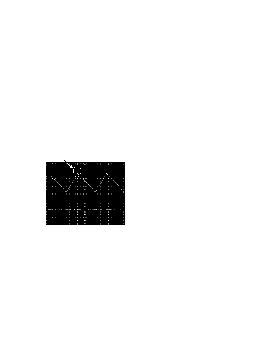
Short Voltage Spikes and How to Reduce Them
The regulator output voltage may also contain short
voltage spikes at the peaks of the sawtooth waveform (see
Figure 26). These voltage spikes are present because of the
fast switching action of the output switch, and the parasitic
inductance of the output filter capacitor. There are some
other important factors such as wiring inductance, stray
capacitance, as well as the scope probe used to evaluate
these transients, all these contribute to the amplitude of these
spikes. To minimize these voltage spikes, low inductance
capacitors should be used, and their lead lengths must be
kept short. The importance of quality printed circuit board
layout design should also be highlighted.
HORIZONTAL TIME BASE: 5.0
s/DIV
VER
TRICAL
RESOLUTION
20
mV/DIV
Voltage spikes caused by switching action of the output
switch and the parasitic inductance of the output capacitor
Figure 26. Output Ripple Voltage Waveforms
Unfiltered
Output
Voltage
Filtered
Output
Voltage
Minimizing the Output Ripple
In order to minimize the output ripple voltage it is possible to
enlarge the inductance value of the inductor L1 and/or to use a
larger value output capacitor. There is also another way to
smooth the output by means of an additional LC filter (20
H,
100
F), that can be added to the output (see Figure 35) to
further reduce the amount of output ripple and transients.
With such a filter it is possible to reduce the output ripple
voltage transients 10 times or more. Figure 26 shows the
difference between filtered and unfiltered output waveforms
of the regulator shown in Figure 34.
The upper waveform is from the normal unfiltered output of
the converter, while the lower waveform shows the output
ripple voltage filtered by an additional LC filter.
Heatsinking and Thermal Considerations
The LM2574 is available in both 8–pin DIP and SO–16L
packages. When used in the typical application the copper lead
frame conducts the majority of the heat from the die, through
the leads, to the printed circuit copper. The copper and the
board are the heatsink for this package and the other heat
producing components, such as the catch diode and inductor.
For the best thermal performance, wide copper traces
should be used and all ground and unused pins should be
soldered to generous amounts of printed circuit board
copper, such as a ground plane. Large areas of copper
provide the best transfer of heat to the surrounding air. One
exception to this is the output (switch) pin, which should not
have large areas of copper in order to minimize coupling to
sensitive circuitry.
Additional improvement in heat dissipation can be
achieved even by using of double sided or multilayer boards
which can provide even better heat path to the ambient.
Using a socket for the 8–pin DIP package is not
recommended because socket represents an additional
thermal resistance, and as a result the junction temperature
will be higher.
Since the current rating of the LM2574 is only 0.5 A, the
total package power dissipation for this switcher is quite low,
ranging from approximately 0.1 W up to 0.75 W under varying
conditions. In a carefully engineered printed circuit board, the
through–hole DIP package can easily dissipate up to 0.75 W,
even at ambient temperatures of 60
°C, and still keep the
maximum junction temperature below 125
°C.
Thermal Analysis and Design
The following procedure must be performed to determine
the operating junction temperature. First determine:
1. PD(max) – maximum regulator power dissipation in the
application.
2. TA(max) – maximum ambient temperature in the
application.
3. TJ(max) – maximum allowed junction temperature
(125
°C for the LM2574). For a conservative
design, the maximum junction temperature
should not exceed 110
°C to assure safe
operation. For every additional +10
°C
temperature rise that the junction must
withstand, the estimated operating lifetime of
the component is halved.
4. R
θJC
– package thermal resistance junction–case.
5. R
θJA
– package thermal resistance junction–ambient.
(Refer to Absolute Maximum Ratings on page 2 of this data
sheet or R
θJC and RθJA values).
The following formula is to calculate the approximate total
power dissipated by the LM2574:
PD = (Vin x IQ) + d x ILoad x Vsat
where d is the duty cycle and for buck converter
d
+
ton
T
+
V
O
V
in
,
IQ (quiescent current) and Vsat can be found in the
LM2574 data sheet,
Vin is minimum input voltage applied,
VO is the regulator output voltage,
ILoad is the load current.
相关PDF资料 |
PDF描述 |
|---|---|
| LM2574N-ADJ | 1.8 A SWITCHING REGULATOR, 63 kHz SWITCHING FREQ-MAX, PDIP8 |
| LM2574DW-ADJR2 | 1.8 A SWITCHING REGULATOR, 63 kHz SWITCHING FREQ-MAX, PDSO16 |
| LM2574N-15 | 1.8 A SWITCHING REGULATOR, 63 kHz SWITCHING FREQ-MAX, PDIP8 |
| LM2575-05IKTTR | 4 A SWITCHING REGULATOR, 63 kHz SWITCHING FREQ-MAX, PSSO5 |
| LM2575-33IKTTR | 4 A SWITCHING REGULATOR, 63 kHz SWITCHING FREQ-MAX, PSSO5 |
相关代理商/技术参数 |
参数描述 |
|---|---|
| LM2574DW-ADJR2 | 功能描述:直流/直流开关调节器 500mA Adj. Step Down RoHS:否 制造商:International Rectifier 最大输入电压:21 V 开关频率:1.5 MHz 输出电压:0.5 V to 0.86 V 输出电流:4 A 输出端数量: 最大工作温度: 安装风格:SMD/SMT 封装 / 箱体:PQFN 4 x 5 |
| LM2574DW-ADJR2G | 功能描述:直流/直流开关调节器 500mA Adj. Step Down RoHS:否 制造商:International Rectifier 最大输入电压:21 V 开关频率:1.5 MHz 输出电压:0.5 V to 0.86 V 输出电流:4 A 输出端数量: 最大工作温度: 安装风格:SMD/SMT 封装 / 箱体:PQFN 4 x 5 |
| LM2574HV | 制造商:NSC 制造商全称:National Semiconductor 功能描述: |
| LM2574HVM-12 | 功能描述:直流/直流开关转换器 RoHS:否 制造商:STMicroelectronics 最大输入电压:4.5 V 开关频率:1.5 MHz 输出电压:4.6 V 输出电流:250 mA 输出端数量:2 最大工作温度:+ 85 C 安装风格:SMD/SMT |
| LM2574HVM-12/NOPB | 功能描述:直流/直流开关转换器 RoHS:否 制造商:STMicroelectronics 最大输入电压:4.5 V 开关频率:1.5 MHz 输出电压:4.6 V 输出电流:250 mA 输出端数量:2 最大工作温度:+ 85 C 安装风格:SMD/SMT |
发布紧急采购,3分钟左右您将得到回复。