- 您现在的位置:买卖IC网 > PDF目录240260 > LM2574HV-12MDC (NATIONAL SEMICONDUCTOR CORP) 1.8 A SWITCHING REGULATOR, 63 kHz SWITCHING FREQ-MAX, UUC PDF资料下载
参数资料
| 型号: | LM2574HV-12MDC |
| 厂商: | NATIONAL SEMICONDUCTOR CORP |
| 元件分类: | 稳压器 |
| 英文描述: | 1.8 A SWITCHING REGULATOR, 63 kHz SWITCHING FREQ-MAX, UUC |
| 封装: | DIE |
| 文件页数: | 11/33页 |
| 文件大小: | 814K |
| 代理商: | LM2574HV-12MDC |
第1页第2页第3页第4页第5页第6页第7页第8页第9页第10页当前第11页第12页第13页第14页第15页第16页第17页第18页第19页第20页第21页第22页第23页第24页第25页第26页第27页第28页第29页第30页第31页第32页第33页
Application Hints (Continued)
The data sheet thermal resistance curves and the thermal
model in
Switchers Made Simple software (version 3.3)
can estimate the maximum junction temperature based on
operating conditions. ln addition, the junction temperature
can be estimated in actual circuit operation by using the fol-
lowing equation.
T
j = Tcu +(θj-cu xPD)
With the switcher operating under worst case conditions and
all other components on the board in the intended enclosure,
measure the copper temperature (T
cu ) near the IC. This can
be done by temporarily soldering a small thermocouple to
the pc board copper near the IC, or by holding a small ther-
mocouple on the pc board copper using thermal grease for
good thermal conduction.
The thermal resistance (
θ
j-cu) for the two packages is:
θ
j-cu = 42C/W for the N-8 package
θ
j-cu = 52C/W for the M-14 package
The power dissipation (P
D) for the IC could be measured, or
it can be estimated by using the formula:
Where I
S is obtained from the typical supply current curve
(adjustable version use the supply current vs. duty cycle
curve).
Additional Applications
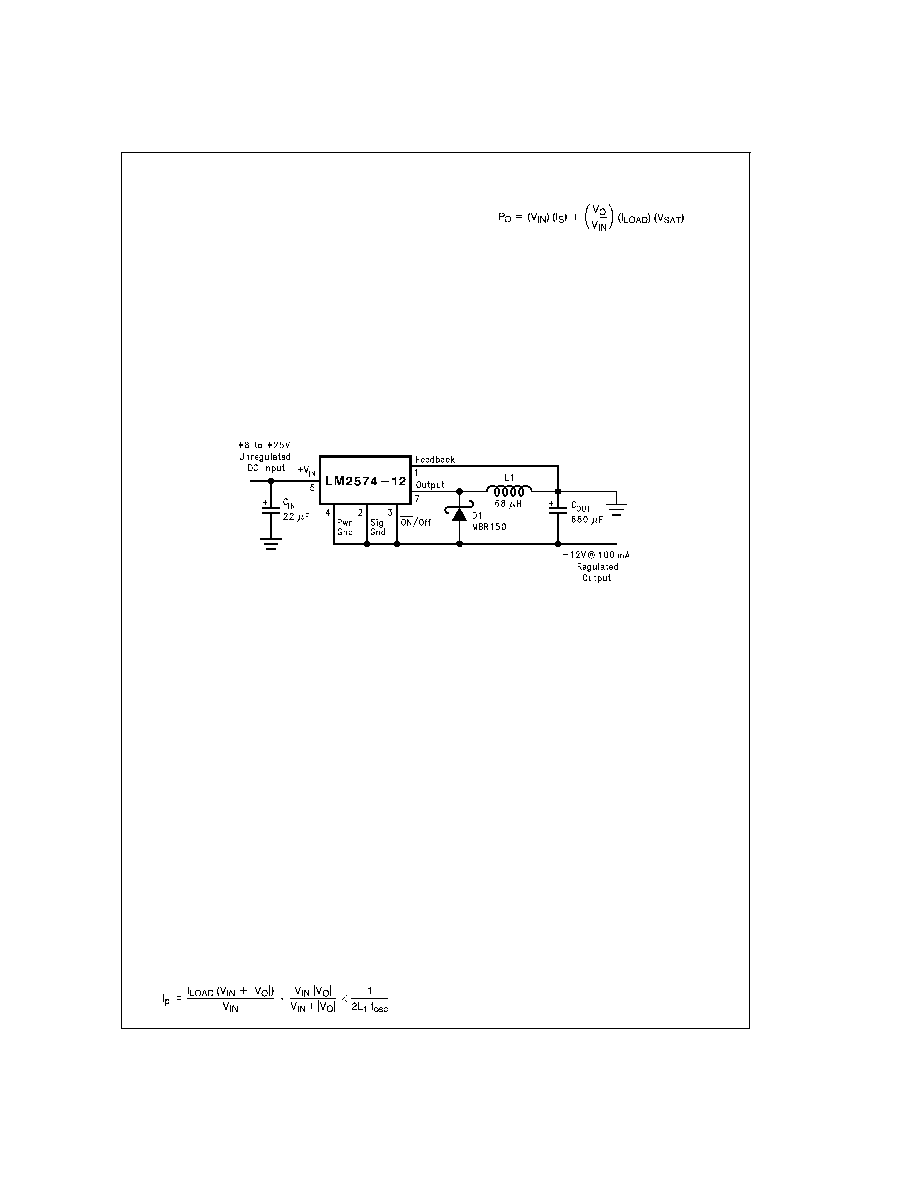
INVERTING REGULATOR
Figure 11 shows a LM2574-12 in a buck-boost configuration
to generate a negative 12V output from a positive input volt-
age. This circuit bootstraps the regulator’s ground pin to the
negative output voltage, then by grounding the feedback pin,
the regulator senses the inverted output voltage and regu-
lates it to 12V.
For an input voltage of 8V or more, the maximum available
output current in this configuration is approximately 100 mA.
At lighter loads, the minimum input voltage required drops to
approximately 4.7V.
The switch currents in this buck-boost configuration are
higher than in the standard buck-mode design, thus lowering
the available output current. Also, the start-up input current
of the buck-boost converter is higher than the standard buck-
mode regulator, and this may overload an input power
source with a current limit less than 0.6A. Using a delayed
turn-on or an undervoltage lockout circuit (described in the
next section) would allow the input voltage to rise to a high
enough level before the switcher would be allowed to turn
on.
Because of the structural differences between the buck and
the buck-boost regulator topologies, the buck regulator de-
sign procedure section can not be used to to select the in-
ductor or the output capacitor. The recommended range of
inductor values for the buck-boost design is between 68 H
and 220 H, and the output capacitor values must be larger
than what is normally required for buck designs. Low input
voltages or high output currents require a large value output
capacitor (in the thousands of micro Farads).
The peak inductor current, which is the same as the peak
switch current, can be calculated from the following formula:
Where f
osc = 52 kHz. Under normal continuous inductor cur-
rent operating conditions, the minimum V
IN represents the
worst case. Select an inductor that is rated for the peak cur-
rent anticipated.
Also, the maximum voltage appearing across the regulator is
the absolute sum of the input and output voltage. For a 12V
output, the maximum input voltage for the LM2574 is +28V,
or +48V for the LM2574HV.
The
Switchers Made Simple version 3.3) design software
can be used to determine the feasibility of regulator designs
using different topologies, different input-output parameters,
different components, etc.
NEGATIVE BOOST REGULATOR
Another variation on the buck-boost topology is the negative
boost configuration. The circuit in
Figure 12 accepts an input
voltage ranging from 5V to 12V and provides a regulated
12V output. Input voltages greater than 12V will cause the
output to rise above 12V, but will not damage the regulator.
DS011394-19
Note: Pin numbers are for the 8-pin DIP package.
FIGURE 11. Inverting Buck-Boost Develops 12V
www.national.com
19
相关PDF资料 |
PDF描述 |
|---|---|
| LES50A48-1V2RE | 1-OUTPUT 60 W DC-DC REG PWR SUPPLY MODULE |
| LES40A48-1V8A | 1-OUTPUT 72 W DC-DC REG PWR SUPPLY MODULE |
| LX1673-09CLQTR | 1 A SWITCHING CONTROLLER, 1035 kHz SWITCHING FREQ-MAX, PQCC20 |
| LES30A48-3V3ANJ | 1-OUTPUT 99 W DC-DC REG PWR SUPPLY MODULE |
| LES40A48-2V5AKJ | 1-OUTPUT 100 W DC-DC REG PWR SUPPLY MODULE |
相关代理商/技术参数 |
参数描述 |
|---|---|
| LM2574HVM-12 | 功能描述:直流/直流开关转换器 RoHS:否 制造商:STMicroelectronics 最大输入电压:4.5 V 开关频率:1.5 MHz 输出电压:4.6 V 输出电流:250 mA 输出端数量:2 最大工作温度:+ 85 C 安装风格:SMD/SMT |
| LM2574HVM-12/NOPB | 功能描述:直流/直流开关转换器 RoHS:否 制造商:STMicroelectronics 最大输入电压:4.5 V 开关频率:1.5 MHz 输出电压:4.6 V 输出电流:250 mA 输出端数量:2 最大工作温度:+ 85 C 安装风格:SMD/SMT |
| LM2574HVM-12/NOPB | 制造商:Texas Instruments 功能描述:DC/DC Converter IC |
| LM2574HVM-15 | 功能描述:直流/直流开关转换器 RoHS:否 制造商:STMicroelectronics 最大输入电压:4.5 V 开关频率:1.5 MHz 输出电压:4.6 V 输出电流:250 mA 输出端数量:2 最大工作温度:+ 85 C 安装风格:SMD/SMT |
| LM2574HVM-15/NOPB | 功能描述:直流/直流开关转换器 RoHS:否 制造商:STMicroelectronics 最大输入电压:4.5 V 开关频率:1.5 MHz 输出电压:4.6 V 输出电流:250 mA 输出端数量:2 最大工作温度:+ 85 C 安装风格:SMD/SMT |
发布紧急采购,3分钟左右您将得到回复。