- 您现在的位置:买卖IC网 > PDF目录13332 > LM2575D2T-015 (ON Semiconductor)IC REG BUCK 15V 1A D2PAK PDF资料下载
参数资料
| 型号: | LM2575D2T-015 |
| 厂商: | ON Semiconductor |
| 文件页数: | 18/28页 |
| 文件大小: | 0K |
| 描述: | IC REG BUCK 15V 1A D2PAK |
| 产品变化通告: | LTB Notification 03/Jan/2008 |
| 标准包装: | 50 |
| 类型: | 降压(降压) |
| 输出类型: | 固定 |
| 输出数: | 1 |
| 输出电压: | 15V |
| 输入电压: | 4.75 V ~ 40 V |
| PWM 型: | 电压模式 |
| 频率 - 开关: | 52kHz |
| 电流 - 输出: | 1A |
| 同步整流器: | 无 |
| 工作温度: | -40°C ~ 125°C |
| 安装类型: | 表面贴装 |
| 封装/外壳: | TO-263-6,D²Pak(5 引线+接片),TO-263BA |
| 包装: | 管件 |
| 供应商设备封装: | D2PAK |
第1页第2页第3页第4页第5页第6页第7页第8页第9页第10页第11页第12页第13页第14页第15页第16页第17页当前第18页第19页第20页第21页第22页第23页第24页第25页第26页第27页第28页
�� �
�
�LM2575,� NCV2575�
�GENERAL� RECOMMENDATIONS�
�Output� Voltage� Ripple� and� Transients�
�Source� of� the� Output� Ripple�
�Since� the� LM2575� is� a� switch� mode� power� supply�
�regulator,� its� output� voltage,� if� left� unfiltered,� will� contain� a�
�sawtooth� ripple� voltage� at� the� switching� frequency.� The�
�output� ripple� voltage� value� ranges� from� 0.5%� to� 3%� of� the�
�output� voltage.� It� is� caused� mainly� by� the� inductor� sawtooth�
�ripple� current� multiplied� by� the� ESR� of� the� output� capacitor.�
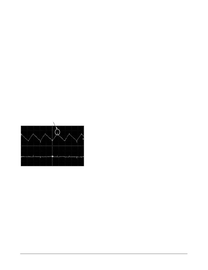
�Short� Voltage� Spikes� and� How� to� Reduce� Them�
�The� regulator� output� voltage� may� also� contain� short�
�voltage� spikes� at� the� peaks� of� the� sawtooth� waveform� (see�
�Figure� 24).� These� voltage� spikes� are� present� because� of� the�
�fast� switching� action� of� the� output� switch,� and� the� parasitic�
�inductance� of� the� output� filter� capacitor.� There� are� some�
�other� important� factors� such� as� wiring� inductance,� stray�
�capacitance,� as� well� as� the� scope� probe� used� to� evaluate� these�
�transients,� all� these� contribute� to� the� amplitude� of� these�
�spikes.� To� minimize� these� voltage� spikes,� low� inductance�
�capacitors� should� be� used,� and� their� lead� lengths� must� be�
�kept� short.� The� importance� of� quality� printed� circuit� board�
�layout� design� should� also� be� highlighted.�
�Voltage� spikes� caused� by� switching� action� of� the� output�
�switch� and� the� parasitic� inductance� of� the� output� capacitor�
�UNFILTERED�
�OUTPUT�
�VOLTAGE�
�VERTICAL�
�Heatsinking� and� Thermal� Considerations�
�The� Through� ?� Hole� Package� TO� ?� 220�
�The� LM2575� is� available� in� two� packages,� a� 5� ?� pin�
�TO� ?� 220(T,� TV)� and� a� 5� ?� pin� surface� mount� D� 2� PAK(D2T).�
�There� are� many� applications� that� require� no� heatsink� to� keep�
�the� LM2575� junction� temperature� within� the� allowed�
�operating� range.� The� TO� ?� 220� package� can� be� used� without�
�a� heatsink� for� ambient� temperatures� up� to� approximately�
�50� °� C� (depending� on� the� output� voltage� and� load� current).�
�Higher� ambient� temperatures� require� some� heatsinking,�
�either� to� the� printed� circuit� (PC)� board� or� an� external�
�heatsink.�
�The� Surface� Mount� Package� D� 2� PAK� and� its�
�Heatsinking�
�The� other� type� of� package,� the� surface� mount� D� 2� PAK,� is�
�designed� to� be� soldered� to� the� copper� on� the� PC� board.� The�
�copper� and� the� board� are� the� heatsink� for� this� package� and�
�the� other� heat� producing� components,� such� as� the� catch�
�diode� and� inductor.� The� PC� board� copper� area� that� the�
�package� is� soldered� to� should� be� at� least� 0.4� in� 2� (or� 100� mm� 2� )�
�and� ideally� should� have� 2� or� more� square� inches� (1300� mm� 2� )�
�of� 0.0028� inch� copper.� Additional� increasing� of� copper� area�
�beyond� approximately� 3.0� in� 2� (2000� mm� 2� )� will� not� improve�
�heat� dissipation� significantly.� If� further� thermal�
�improvements� are� needed,� double� sided� or� multilayer� PC�
�boards� with� large� copper� areas� should� be� considered.�
�Thermal� Analysis� and� Design�
�The� following� procedure� must� be� performed� to� determine�
�whether� or� not� a� heatsink� will� be� required.� First� determine:�
�RESOLUTION:�
�20� mV/DIV�
�1.� P� D(max)�
�maximum� regulator� power� dissipation� in�
�the� application.�
�FILTERED�
�OUTPUT�
�VOLTAGE�
�HORIZONTAL� TIME� BASE:� 10� m� s/DIV�
�Figure� 24.� Output� Ripple� Voltage� Waveforms�
�Minimizing� the� Output� Ripple�
�In� order� to� minimize� the� output� ripple� voltage� it� is� possible�
�to� enlarge� the� inductance� value� of� the� inductor� L1� and/or� to�
�use� a� larger� value� output� capacitor.� There� is� also� another� way�
�to� smooth� the� output� by� means� of� an� additional� LC� filter�
�(20� m� H,� 100� m� F),� that� can� be� added� to� the� output� (see�
�Figure� 33)� to� further� reduce� the� amount� of� output� ripple� and�
�transients.� With� such� a� filter� it� is� possible� to� reduce� the�
�output� ripple� voltage� transients� 10� times� or� more.� Figure� 24�
�shows� the� difference� between� filtered� and� unfiltered� output�
�waveforms� of� the� regulator� shown� in� Figure� 33.�
�The� upper� waveform� is� from� the� normal� unfiltered� output�
�of� the� converter,� while� the� lower� waveform� shows� the� output�
�2.� T� A(max� )� maximum� ambient� temperature� in� the�
�application.�
�3.� T� J(max)� maximum� allowed� junction� temperature�
�(125� °� C� for� the� LM2575).� For� a� conservative�
�design,� the� maximum� junction� temperature�
�should� not� exceed� 110� °� C� to� assure� safe�
�operation.� For� every� additional� 10� °� C�
�temperature� rise� that� the� junction� must�
�withstand,� the� estimated� operating� lifetime�
�of� the� component� is� halved.�
�4.� R� q� JC� package� thermal� resistance� junction� ?� case.�
�5.� R� q� JA� package� thermal� resistance� junction� ?� ambient.�
�(Refer� to� Absolute� Maximum� Ratings� in� this� data� sheet� or�
�R� q� JC� and� R� q� JA� values).�
�The� following� formula� is� to� calculate� the� total� power�
�dissipated� by� the� LM2575:�
�P� D� =� (V� in� x� I� Q� )� +� d� x� I� Load� x� V� sat�
�where� d� is� the� duty� cycle� and� for� buck� converter�
�ripple� voltage� filtered� by� an� additional� LC� filter.�
�http://onsemi.com�
�18�
�相关PDF资料 |
PDF描述 |
|---|---|
| VI-2V1-EX-F2 | CONVERTER MOD DC/DC 12V 75W |
| BU31TA2WNVX-TR | IC REG LDO 3.1V .2A 4-SSON |
| LM2575D2T-012G | IC REG BUCK 12V 1A D2PAK |
| VI-2V1-EX-F1 | CONVERTER MOD DC/DC 12V 75W |
| VI-2TY-EV-F3 | CONVERTER MOD DC/DC 3.3V 99W |
相关代理商/技术参数 |
参数描述 |
|---|---|
| LM2575D2T-015G | 功能描述:直流/直流开关调节器 15V 1A Buck PWM RoHS:否 制造商:International Rectifier 最大输入电压:21 V 开关频率:1.5 MHz 输出电压:0.5 V to 0.86 V 输出电流:4 A 输出端数量: 最大工作温度: 安装风格:SMD/SMT 封装 / 箱体:PQFN 4 x 5 |
| LM2575D2T-12 | 制造商:MOTOROLA 制造商全称:Motorola, Inc 功能描述:EASY SWITCHERE⑩ 1.0 A STEP-DOWN VOLTAGE REGULATOR |
| LM2575D2T-12R4 | 功能描述:直流/直流开关调节器 12V 1A Buck PWM RoHS:否 制造商:International Rectifier 最大输入电压:21 V 开关频率:1.5 MHz 输出电压:0.5 V to 0.86 V 输出电流:4 A 输出端数量: 最大工作温度: 安装风格:SMD/SMT 封装 / 箱体:PQFN 4 x 5 |
| LM2575D2T-12R4G | 功能描述:直流/直流开关调节器 12V 1A Buck PWM RoHS:否 制造商:International Rectifier 最大输入电压:21 V 开关频率:1.5 MHz 输出电压:0.5 V to 0.86 V 输出电流:4 A 输出端数量: 最大工作温度: 安装风格:SMD/SMT 封装 / 箱体:PQFN 4 x 5 |
| LM2575D2T-15 | 制造商:MOTOROLA 制造商全称:Motorola, Inc 功能描述:EASY SWITCHERE⑩ 1.0 A STEP-DOWN VOLTAGE REGULATOR |
发布紧急采购,3分钟左右您将得到回复。