- 您现在的位置:买卖IC网 > PDF目录79926 > LM2575HVS-12EP (NATIONAL SEMICONDUCTOR CORP) 3.2 A SWITCHING REGULATOR, 63 kHz SWITCHING FREQ-MAX, PSSO5 PDF资料下载
参数资料
| 型号: | LM2575HVS-12EP |
| 厂商: | NATIONAL SEMICONDUCTOR CORP |
| 元件分类: | 稳压器 |
| 英文描述: | 3.2 A SWITCHING REGULATOR, 63 kHz SWITCHING FREQ-MAX, PSSO5 |
| 封装: | TO-263, 5 PIN |
| 文件页数: | 25/26页 |
| 文件大小: | 1069K |
| 代理商: | LM2575HVS-12EP |
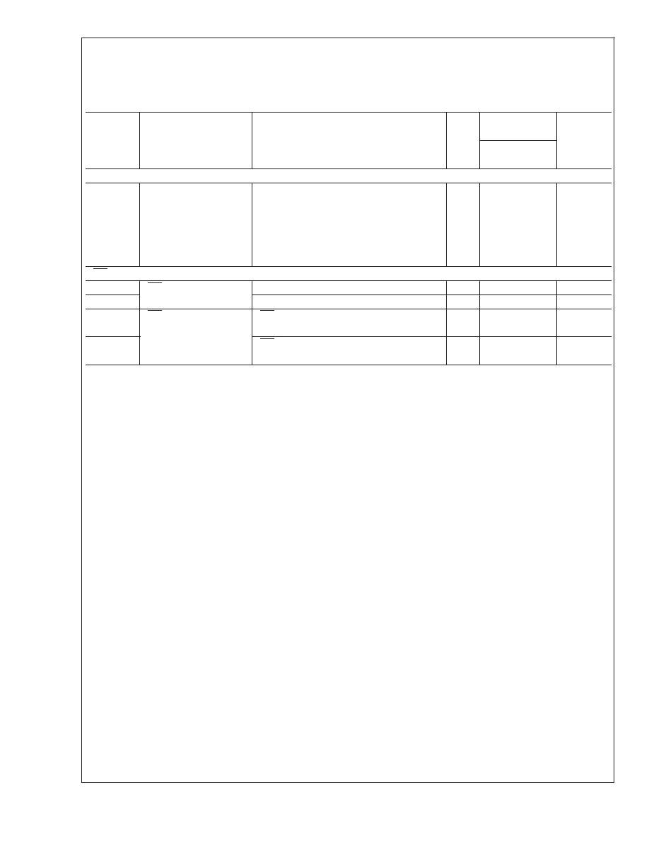
All Output Voltage Versions
Electrical Characteristics (Note 16) (Continued)
Specifications with standard type face are for T
J = 25C, and those with boldface type apply over full Operating Tempera-
ture Range. Unless otherwise specified, V
IN = 12V for the 3.3V, 5V, and Adjustable version, VIN = 25V for the 12V version,
and V
IN = 30V for the 15V version. ILOAD = 200 mA.
Symbol
Parameter
Conditions
Typ
LM2575-XXEP
Units
(Limits)
LM2575HV-XXEP
Limit
DEVICE PARAMETERS
θ
JA
Thermal Resistance
T Package, Junction to Ambient (Note 11)
65
θ
JA
T Package, Junction to Ambient (Note 12)
45
C/W
θ
JC
T Package, Junction to Case
2
θ
JA
N Package, Junction to Ambient (Note 13)
85
θ
JA
M Package, Junction to Ambient (Note 13)
100
θ
JA
S Package, Junction to Ambient (Note 14)
37
ON /OFF CONTROL Test Circuit Figure 2
V
IH
ON /OFF Pin Logic
V
OUT = 0V
1.4
2.2/2.4
V(Min)
V
IL
Input Level
V
OUT = Nominal Output Voltage
1.2
1.0/0.8
V(Max)
I
IH
ON /OFF Pin Input
ON /OFF Pin = 5V (OFF)
12
A
Current
30
A(Max)
I
IL
ON /OFF Pin = 0V (ON)
0A
10
A(Max)
Note 4: Absolute Maximum Ratings indicate limits beyond which damage to the device may occur. Operating Ratings indicate conditions for which the device is
intended to be functional, but do not guarantee specific performance limits. For guaranteed specifications and test conditions, see the Electrical Characteristics.
Note 5: All limits guaranteed at room temperature (standard type face) and at temperature extremes (bold type face). All room temperature limits are 100%
production tested. All limits at temperature extremes are guaranteed via correlation using standard Statistical Quality Control (SQC) methods.
Note 6: External components such as the catch diode, inductor, input and output capacitors can affect switching regulator system performance. When the
LM2575EP is used as shown in the Figure 2 test circuit, system performance will be as shown in system parameters section of Electrical Characteristics.
Note 7: Output (pin 2) sourcing current. No diode, inductor or capacitor connected to output pin.
Note 8: Feedback (pin 4) removed from output and connected to 0V.
Note 9: Feedback (pin 4) removed from output and connected to +12V for the Adjustable, 3.3V, and 5V versions, and +25V for the 12V and 15V versions, to force
the output transistor OFF.
Note 10: VIN = 40V (60V for the high voltage version).
Note 11: Junction to ambient thermal resistance (no external heat sink) for the 5 lead TO-220 package mounted vertically, with 12 inch leads in a socket, or on a
PC board with minimum copper area.
Note 12: Junction to ambient thermal resistance (no external heat sink) for the 5 lead TO-220 package mounted vertically, with 12 inch leads soldered to a PC board
containing approximately 4 square inches of copper area surrounding the leads.
Note 13: Junction to ambient thermal resistance with approximately 1 square inch of pc board copper surrounding the leads. Additional copper area will lower
thermal resistance further. See thermal model in Switchers made Simple software.
Note 14: If the TO-263 package is used, the thermal resistance can be reduced by increasing the PC board copper area thermally connected to the package: Using
0.5 square inches of copper area,
θJA is 50C/W; with 1 square inch of copper area, θJA is 37C/W; and with 1.6 or more square inches of copper area, θJA is 32C/W.
Note 15: The oscillator frequency reduces to approximately 18 kHz in the event of an output short or an overload which causes the regulated output voltage to drop
approximately 40% from the nominal output voltage. This self protection feature lowers the average power dissipation of the IC by lowering the minimum duty cycle
from 5% down to approximately 2%.
Note 16: "Testing and other quality control techniques are used to the extent deemed necessary to ensure product performance over the specified temperature
range. Product may not necessarily be tested across the full temperature range and all parameters may not necessarily be tested. In the absence of specific
PARAMETRIC testing, product performance is assured by characterization and/or design."
LM2575EP/LM2575HVEP
www.national.com
8
相关PDF资料 |
PDF描述 |
|---|---|
| LTC3872ETS8#PBF | SWITCHING CONTROLLER, 650 kHz SWITCHING FREQ-MAX, PDSO8 |
| LTC3850EGN | 0.1 A DUAL SWITCHING CONTROLLER, 860 kHz SWITCHING FREQ-MAX, PDSO28 |
| LT1933HS6#TR | 1.05 A SWITCHING REGULATOR, 600 kHz SWITCHING FREQ-MAX, PDSO6 |
| LC016AJ | 2-OUTPUT 16 W DC-DC REG PWR SUPPLY MODULE |
| LTC4224CMS-2#PBF | 2-CHANNEL POWER SUPPLY SUPPORT CKT, PDSO10 |
相关代理商/技术参数 |
参数描述 |
|---|---|
| LM2575HVS-15 | 功能描述:直流/直流开关转换器 RoHS:否 制造商:STMicroelectronics 最大输入电压:4.5 V 开关频率:1.5 MHz 输出电压:4.6 V 输出电流:250 mA 输出端数量:2 最大工作温度:+ 85 C 安装风格:SMD/SMT |
| LM2575HVS-15/NOPB | 功能描述:直流/直流开关转换器 RoHS:否 制造商:STMicroelectronics 最大输入电压:4.5 V 开关频率:1.5 MHz 输出电压:4.6 V 输出电流:250 mA 输出端数量:2 最大工作温度:+ 85 C 安装风格:SMD/SMT |
| LM2575HVS-15/NOPB | 制造商:Texas Instruments 功能描述:DC/DC Converter IC |
| LM2575HVS-3.3 | 功能描述:直流/直流开关转换器 RoHS:否 制造商:STMicroelectronics 最大输入电压:4.5 V 开关频率:1.5 MHz 输出电压:4.6 V 输出电流:250 mA 输出端数量:2 最大工作温度:+ 85 C 安装风格:SMD/SMT |
| LM2575HVS-3.3/NOPB | 功能描述:直流/直流开关转换器 1A STEP-DOWN VLTG REG RoHS:否 制造商:STMicroelectronics 最大输入电压:4.5 V 开关频率:1.5 MHz 输出电压:4.6 V 输出电流:250 mA 输出端数量:2 最大工作温度:+ 85 C 安装风格:SMD/SMT |
发布紧急采购,3分钟左右您将得到回复。