- 您现在的位置:买卖IC网 > PDF目录44549 > LM2588-ADJMWC (NATIONAL SEMICONDUCTOR CORP) 9.5 A SWITCHING REGULATOR, 200 kHz SWITCHING FREQ-MAX, UUC PDF资料下载
参数资料
| 型号: | LM2588-ADJMWC |
| 厂商: | NATIONAL SEMICONDUCTOR CORP |
| 元件分类: | 稳压器 |
| 英文描述: | 9.5 A SWITCHING REGULATOR, 200 kHz SWITCHING FREQ-MAX, UUC |
| 封装: | WAFER |
| 文件页数: | 18/33页 |
| 文件大小: | 863K |
| 代理商: | LM2588-ADJMWC |
第1页第2页第3页第4页第5页第6页第7页第8页第9页第10页第11页第12页第13页第14页第15页第16页第17页当前第18页第19页第20页第21页第22页第23页第24页第25页第26页第27页第28页第29页第30页第31页第32页第33页
Application Hints (Continued)
SWITCH VOLTAGE LIMITS
In a flyback regulator, the maximum steady-state voltage ap-
pearing at the switch, when it is off, is set by the transformer
turns ratio, N, the output voltage, V
OUT, and the maximum in-
put voltage, V
IN (Max):
V
SW(OFF) = VIN (Max) + (VOUT +VF)/N
where V
F is the forward biased voltage of the output diode,
and is typically 0.5V for Schottky diodes and 0.8V for
ultra-fast recovery diodes. In certain circuits, there exists a
voltage spike, V
LL, superimposed on top of the steady-state
voltage (see
Figure 5, waveform A). Usually, this voltage
spike is caused by the transformer leakage inductance
and/or the output rectifier recovery time. To “clamp” the volt-
age at the switch from exceeding its maximum value, a tran-
sient suppressor in series with a diode is inserted across the
transformer primary (as shown in the circuit in
Figure 4 and
other flyback regulator circuits throughout the datasheet).
The schematic in
Figure 46 shows another method of clamp-
ing the switch voltage. A single voltage transient suppressor
(the SA51A) is inserted at the switch pin. This method
clamps the total voltage across the switch, not just the volt-
age across the primary.
If poor circuit layout techniques are used (see the “Circuit
Layout Guideline” section), negative voltage transients may
appear on the Switch pin (pin 5). Applying a negative voltage
(with respect to the IC’s ground) to any monolithic IC pin
causes erratic and unpredictable operation of that IC. This
holds true for the LM2588 IC as well. When used in a flyback
regulator, the voltage at the Switch pin (pin 5) can go nega-
tive when the switch turns on. The “ringing” voltage at the
switch pin is caused by the output diode capacitance and the
transformer leakage inductance forming a resonant circuit at
the secondary(ies). The resonant circuit generates the “ring-
ing” voltage, which gets reflected back through the trans-
former to the switch pin. There are two common methods to
avoid this problem. One is to add an RC snubber around the
output rectifier(s), as in
Figure 46. The values of the resistor
and the capacitor must be chosen so that the voltage at the
Switch pin does not drop below 0.4V. The resistor may
range in value between 10
and1k, and the capacitor will
vary from 0.001 F to 0.1 F. Adding a snubber will (slightly)
reduce the efficiency of the overall circuit.
The other method to reduce or eliminate the “ringing” is to in-
sert a Schottky diode clamp between pins 5 and 4 (ground),
also shown in
Figure 46. This prevents the voltage at pin 5
from dropping below 0.4V. The reverse voltage rating of the
diode must be greater than the switch off voltage.
OUTPUT VOLTAGE LIMITATIONS
The maximum output voltage of a boost regulator is the
maximum switch voltage minus a diode drop. In a flyback
regulator, the maximum output voltage is determined by the
turns ratio, N, and the duty cycle, D, by the equation:
V
OUT ≈ NxVIN xD/(1D)
The duty cycle of a flyback regulator is determined by the fol-
lowing equation:
Theoretically, the maximum output voltage can be as large
as desired — just keep increasing the turns ratio of the trans-
former. However, there exists some physical limitations that
prevent the turns ratio, and thus the output voltage, from in-
creasing to infinity. The physical limitations are capacitances
and inductances in the LM2588 switch, the output diode(s),
and the transformer — such as reverse recovery time of the
output diode (mentioned above).
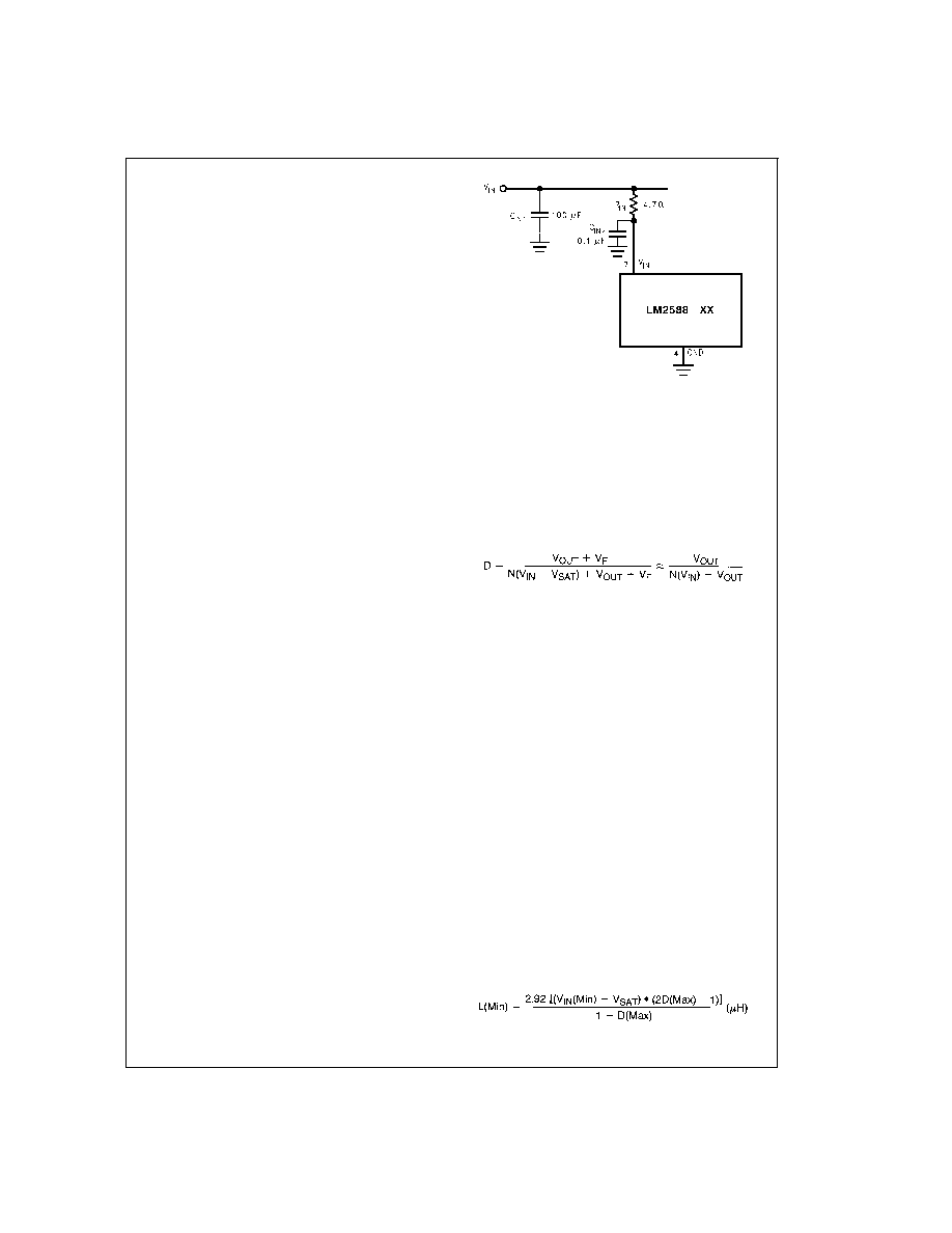
NOISY INPUT LINE CONDITION
A small, low-pass RC filter should be used at the input pin of
the LM2588 if the input voltage has an unusually large
amount of transient noise, such as with an input switch that
bounces. The circuit in
Figure 47 demonstrates the layout of
the filter, with the capacitor placed from the input pin to
ground and the resistor placed between the input supply and
the input pin. Note that the values of R
IN and CIN shown in
the schematic are good enough for most applications, but
some readjusting might be required for a particular applica-
tion. If efficiency is a major concern, replace the resistor with
a small inductor (say 10 H and rated at 200 mA).
STABILITY
All current-mode controlled regulators can suffer from an in-
stability, known as subharmonic oscillation, if they operate
with a duty cycle above 50%. To eliminate subharmonic os-
cillations, a minimum value of inductance is required to en-
sure stability for all boost and flyback regulators. The mini-
mum inductance is given by:
where V
SAT is the switch saturation voltage and can be
found in the Characteristic Curves.
DS012420-58
FIGURE 47. Input Line Filter
www.national.com
25
相关PDF资料 |
PDF描述 |
|---|---|
| LM2588T-12/NOPB | 9.5 A SWITCHING REGULATOR, 200 kHz SWITCHING FREQ-MAX, PSFM7 |
| LM2590HV3.3MDC | 3 A SWITCHING REGULATOR, 173 kHz SWITCHING FREQ-MAX, UUC |
| LM2594-12MDC | 1.4 A SWITCHING REGULATOR, 173 kHz SWITCHING FREQ-MAX, UUC |
| LM2594-5.0MWC | 1.4 A SWITCHING REGULATOR, 173 kHz SWITCHING FREQ-MAX, UUC |
| LM2594-ADJMDC | 1.4 A SWITCHING REGULATOR, 173 kHz SWITCHING FREQ-MAX, UUC |
相关代理商/技术参数 |
参数描述 |
|---|---|
| LM2588S-12 | 功能描述:直流/直流开关转换器 RoHS:否 制造商:STMicroelectronics 最大输入电压:4.5 V 开关频率:1.5 MHz 输出电压:4.6 V 输出电流:250 mA 输出端数量:2 最大工作温度:+ 85 C 安装风格:SMD/SMT |
| LM2588S-12/NOPB | 功能描述:直流/直流开关转换器 RoHS:否 制造商:STMicroelectronics 最大输入电压:4.5 V 开关频率:1.5 MHz 输出电压:4.6 V 输出电流:250 mA 输出端数量:2 最大工作温度:+ 85 C 安装风格:SMD/SMT |
| LM2588S-3.3 | 功能描述:直流/直流开关转换器 RoHS:否 制造商:STMicroelectronics 最大输入电压:4.5 V 开关频率:1.5 MHz 输出电压:4.6 V 输出电流:250 mA 输出端数量:2 最大工作温度:+ 85 C 安装风格:SMD/SMT |
| LM2588S-3.3/NOPB | 功能描述:直流/直流开关转换器 RoHS:否 制造商:STMicroelectronics 最大输入电压:4.5 V 开关频率:1.5 MHz 输出电压:4.6 V 输出电流:250 mA 输出端数量:2 最大工作温度:+ 85 C 安装风格:SMD/SMT |
| LM2588S-5.0 | 功能描述:直流/直流开关转换器 RoHS:否 制造商:STMicroelectronics 最大输入电压:4.5 V 开关频率:1.5 MHz 输出电压:4.6 V 输出电流:250 mA 输出端数量:2 最大工作温度:+ 85 C 安装风格:SMD/SMT |
发布紧急采购,3分钟左右您将得到回复。