- 您现在的位置:买卖IC网 > PDF目录14583 > LM2588S-3.3/NOPB (National Semiconductor)IC REG MULTI CONFIG 3.3V TO263-7 PDF资料下载
参数资料
| 型号: | LM2588S-3.3/NOPB |
| 厂商: | National Semiconductor |
| 文件页数: | 26/38页 |
| 文件大小: | 0K |
| 描述: | IC REG MULTI CONFIG 3.3V TO263-7 |
| 产品培训模块: | SIMPLE SWITCHER® Regulators |
| 标准包装: | 45 |
| 系列: | SIMPLE SWITCHER® |
| 类型: | 升压(升压),回扫,正向转换器 |
| 输出类型: | 固定 |
| 输出数: | 1 |
| 输出电压: | 3.3V |
| 输入电压: | 4 V ~ 40 V |
| PWM 型: | 电流模式 |
| 频率 - 开关: | 100kHz ~ 200kHz |
| 电流 - 输出: | 5A |
| 同步整流器: | 无 |
| 工作温度: | -40°C ~ 125°C |
| 安装类型: | 表面贴装 |
| 封装/外壳: | TO-263-8,D²Pak(7 引线+接片),TO-263CA |
| 包装: | 管件 |
| 供应商设备封装: | TO-263-7 |
| 产品目录页面: | 1304 (CN2011-ZH PDF) |
| 配用: | 551011367-051-ND - BOARD WEBENCH BUILD IT LM2586/88 |
| 其它名称: | *LM2588S-3.3 *LM2588S-3.3/NOPB LM2588S-3.3 |
第1页第2页第3页第4页第5页第6页第7页第8页第9页第10页第11页第12页第13页第14页第15页第16页第17页第18页第19页第20页第21页第22页第23页第24页第25页当前第26页第27页第28页第29页第30页第31页第32页第33页第34页第35页第36页第37页第38页
�� ��
��
��SNVS117D� –� APRIL� 1998� –� REVISED� APRIL� 2013�
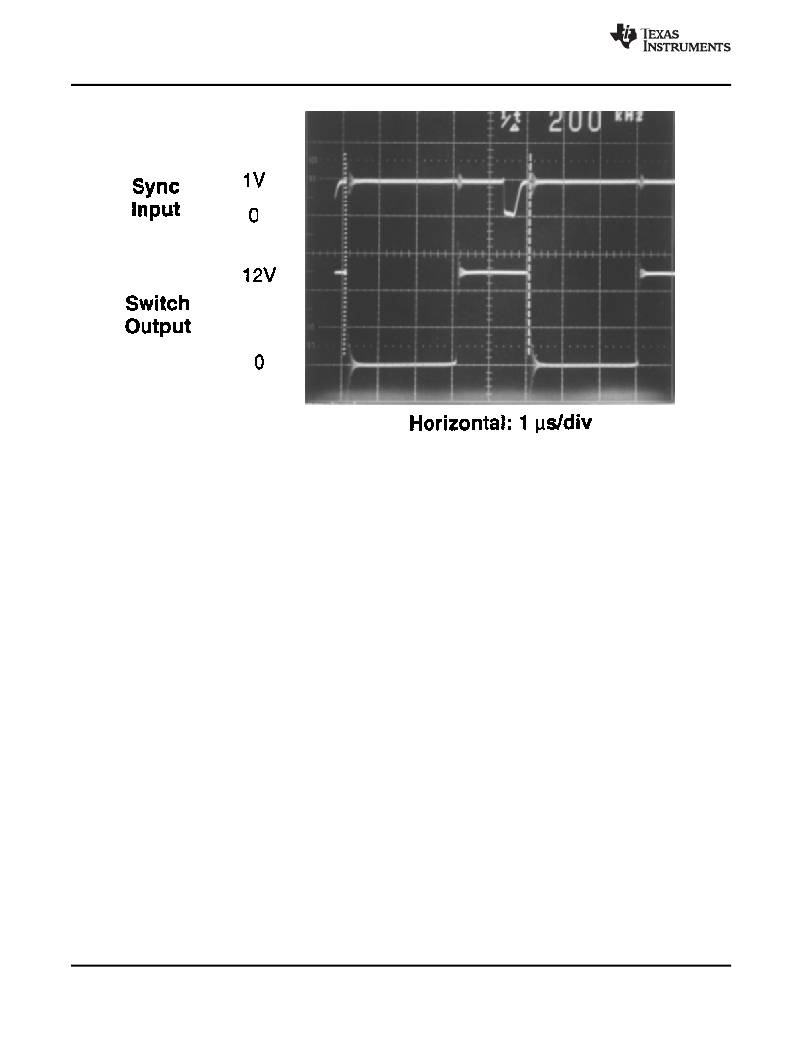
��Figure� 56.� Waveforms� of� a� Synchronized�
�12V� Boost� Regulator�
�The� scope� photo� in� Figure� 56� shows� a� LM2588� 12V� Boost� Regulator� synchronized� to� a� 200� kHz� signal.� There� is�
�a� 700� ns� delay� between� the� falling� edge� of� the� sync� signal� and� the� turning� on� of� the� switch.�
�PROGRAMMING� OUTPUT� VOLTAGE�
�(SELECTING� R1� AND� R2)�
�Referring� to� the� adjustable� regulator� in� Figure� 57� ,� the� output� voltage� is� programmed� by� the� resistors� R1� and� R2�
�by� the� following� formula:�
�V� OUT� =� V� REF� (1� +� R1/R2)�
�where� V� REF� =� 1.23V�
�(1)�
�Resistors� R1� and� R2� divide� the� output� voltage� down� so� that� it� can� be� compared� with� the� 1.23V� internal�
�reference.� With� R2� between� 1k� and� 5k,� R1� is:�
�R1� =� R2� (V� OUT� /V� REF� ?� 1)�
�where� V� REF� =� 1.23V�
�(2)�
�For� best� temperature� coefficient� and� stability� with� time,� use� 1%� metal� film� resistors.�
�SHORT� CIRCUIT� CONDITION�
�Due� to� the� inherent� nature� of� boost� regulators,� when� the� output� is� shorted� (see� Figure� 57� ),� current� flows� directly�
�from� the� input,� through� the� inductor� and� the� diode,� to� the� output,� bypassing� the� switch.� The� current� limit� of� the�
�switch� does� not� limit� the� output� current� for� the� entire� circuit.� To� protect� the� load� and� prevent� damage� to� the�
�switch,� the� current� must� be� externally� limited,� either� by� the� input� supply� or� at� the� output� with� an� external� current�
�limit� circuit.� The� external� limit� should� be� set� to� the� maximum� switch� current� of� the� device,� which� is� 5A.�
�In� a� flyback� regulator� application� (� Figure� 58� ),� using� the� standard� transformers,� the� LM2588� will� survive� a� short�
�circuit� to� the� main� output.� When� the� output� voltage� drops� to� 80%� of� its� nominal� value,� the� frequency� will� drop� to�
�25� kHz.� With� a� lower� frequency,� off� times� are� larger.� With� the� longer� off� times,� the� transformer� can� release� all� of�
�its� stored� energy� before� the� switch� turns� back� on.� Hence,� the� switch� turns� on� initially� with� zero� current� at� its�
�collector.� In� this� condition,� the� switch� current� limit� will� limit� the� peak� current,� saving� the� device.�
�26�
��Product� Folder� Links:� LM2588�
�Copyright� ?� 1998–2013,� Texas� Instruments� Incorporated�
�相关PDF资料 |
PDF描述 |
|---|---|
| MAX6468US25D7+T | IC MPU/RESET CIRC 2.500V SOT143 |
| MAX6468US26D7+T | IC MPU/RESET CIRC 2.625V SOT143 |
| LM2588S-ADJ/NOPB | IC REG MULTI CONFIG ADJ TO263-7 |
| LM2588S-12/NOPB | IC REG MULTI CONFIG 12V TO263-7 |
| MAX6468US27D7+T | IC MPU/RESET CIRC 2.70V SOT143-4 |
相关代理商/技术参数 |
参数描述 |
|---|---|
| LM2588S-5.0 | 功能描述:直流/直流开关转换器 RoHS:否 制造商:STMicroelectronics 最大输入电压:4.5 V 开关频率:1.5 MHz 输出电压:4.6 V 输出电流:250 mA 输出端数量:2 最大工作温度:+ 85 C 安装风格:SMD/SMT |
| LM2588S-5.0/NOPB | 功能描述:直流/直流开关转换器 RoHS:否 制造商:STMicroelectronics 最大输入电压:4.5 V 开关频率:1.5 MHz 输出电压:4.6 V 输出电流:250 mA 输出端数量:2 最大工作温度:+ 85 C 安装风格:SMD/SMT |
| LM2588SADJ | 制造商:National Semiconductor 功能描述:Conv DC-DC Single Step Up 4V to 40V 8-Pin(7+Tab) TO-263 Rail |
| LM2588S-ADJ | 功能描述:直流/直流开关转换器 RoHS:否 制造商:STMicroelectronics 最大输入电压:4.5 V 开关频率:1.5 MHz 输出电压:4.6 V 输出电流:250 mA 输出端数量:2 最大工作温度:+ 85 C 安装风格:SMD/SMT |
| LM2588S-ADJ/NOPB | 功能描述:直流/直流开关转换器 5A FLYBACK REGULATOR RoHS:否 制造商:STMicroelectronics 最大输入电压:4.5 V 开关频率:1.5 MHz 输出电压:4.6 V 输出电流:250 mA 输出端数量:2 最大工作温度:+ 85 C 安装风格:SMD/SMT |
发布紧急采购,3分钟左右您将得到回复。