- 您现在的位置:买卖IC网 > PDF目录14583 > LM2588S-ADJ/NOPB (National Semiconductor)IC REG MULTI CONFIG ADJ TO263-7 PDF资料下载
参数资料
| 型号: | LM2588S-ADJ/NOPB |
| 厂商: | National Semiconductor |
| 文件页数: | 28/38页 |
| 文件大小: | 0K |
| 描述: | IC REG MULTI CONFIG ADJ TO263-7 |
| 产品培训模块: | SIMPLE SWITCHER® Regulators |
| 标准包装: | 45 |
| 系列: | SIMPLE SWITCHER® |
| 类型: | 升压(升压),回扫,正向转换器 |
| 输出类型: | 可调式 |
| 输出数: | 1 |
| 输出电压: | 可调 |
| 输入电压: | 4 V ~ 40 V |
| PWM 型: | 电流模式 |
| 频率 - 开关: | 100kHz ~ 200kHz |
| 电流 - 输出: | 5A |
| 同步整流器: | 无 |
| 工作温度: | -40°C ~ 125°C |
| 安装类型: | 表面贴装 |
| 封装/外壳: | TO-263-8,D²Pak(7 引线+接片),TO-263CA |
| 包装: | 管件 |
| 供应商设备封装: | TO-263-7 |
| 产品目录页面: | 1304 (CN2011-ZH PDF) |
| 配用: | 551011367-051-ND - BOARD WEBENCH BUILD IT LM2586/88 |
| 其它名称: | *LM2588S-ADJ LM2588S-ADJ |
第1页第2页第3页第4页第5页第6页第7页第8页第9页第10页第11页第12页第13页第14页第15页第16页第17页第18页第19页第20页第21页第22页第23页第24页第25页第26页第27页当前第28页第29页第30页第31页第32页第33页第34页第35页第36页第37页第38页
�� ��
��
��SNVS117D� –� APRIL� 1998� –� REVISED� APRIL� 2013�
��where� V� F� is� the� forward� biased� voltage� of� the� output� diode,� and� is� typically� 0.5V� for� Schottky� diodes� and� 0.8V� for�
�ultra-fast� recovery� diodes.� In� certain� circuits,� there� exists� a� voltage� spike,� V� LL� ,� superimposed� on� top� of� the�
�steady-state� voltage� (see� Figure� 21� ,� waveform� A).� Usually,� this� voltage� spike� is� caused� by� the� transformer�
�leakage� inductance� and/or� the� output� rectifier� recovery� time.� To� “clamp”� the� voltage� at� the� switch� from� exceeding�
�its� maximum� value,� a� transient� suppressor� in� series� with� a� diode� is� inserted� across� the� transformer� primary� (as�
�shown� in� the� circuit� in� Figure� 20� and� other� flyback� regulator� circuits� throughout� the� datasheet).� The� schematic� in�
�Figure� 58� shows� another� method� of� clamping� the� switch� voltage.� A� single� voltage� transient� suppressor� (the�
�SA51A)� is� inserted� at� the� switch� pin.� This� method� clamps� the� total� voltage� across� the� switch,� not� just� the� voltage�
�across� the� primary.�
�If� poor� circuit� layout� techniques� are� used� (see� the� CIRCUIT� LAYOUT� GUIDELINES� section),� negative� voltage�
�transients� may� appear� on� the� Switch� pin� (pin� 5).� Applying� a� negative� voltage� (with� respect� to� the� IC's� ground)� to�
�any� monolithic� IC� pin� causes� erratic� and� unpredictable� operation� of� that� IC.� This� holds� true� for� the� LM2588� IC� as�
�well.� When� used� in� a� flyback� regulator,� the� voltage� at� the� Switch� pin� (pin� 5)� can� go� negative� when� the� switch�
�turns� on.� The� “ringing”� voltage� at� the� switch� pin� is� caused� by� the� output� diode� capacitance� and� the� transformer�
�leakage� inductance� forming� a� resonant� circuit� at� the� secondary(ies).� The� resonant� circuit� generates� the� “ringing”�
�voltage,� which� gets� reflected� back� through� the� transformer� to� the� switch� pin.� There� are� two� common� methods� to�
�avoid� this� problem.� One� is� to� add� an� RC� snubber� around� the� output� rectifier(s),� as� in� Figure� 58� .� The� values� of� the�
�resistor� and� the� capacitor� must� be� chosen� so� that� the� voltage� at� the� Switch� pin� does� not� drop� below� ?� 0.4V.� The�
�resistor� may� range� in� value� between� 10� Ω� and� 1� k� Ω� ,� and� the� capacitor� will� vary� from� 0.001� μ� F� to� 0.1� μ� F.� Adding� a�
�snubber� will� (slightly)� reduce� the� efficiency� of� the� overall� circuit.�
�The� other� method� to� reduce� or� eliminate� the� “ringing”� is� to� insert� a� Schottky� diode� clamp� between� pins� 5� and� 4�
�(ground),� also� shown� in� Figure� 58� .� This� prevents� the� voltage� at� pin� 5� from� dropping� below� ?� 0.4V.� The� reverse�
�voltage� rating� of� the� diode� must� be� greater� than� the� switch� off� voltage.�
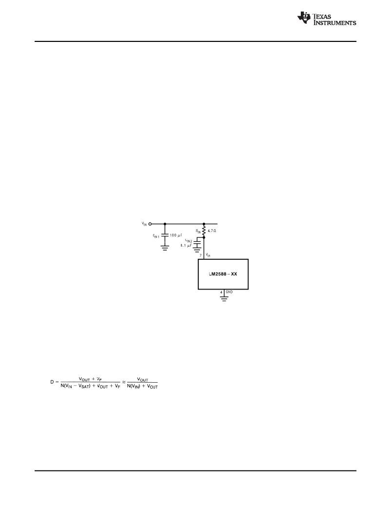
�Figure� 59.� Input� Line� Filter�
�OUTPUT� VOLTAGE� LIMITATIONS�
�The� maximum� output� voltage� of� a� boost� regulator� is� the� maximum� switch� voltage� minus� a� diode� drop.� In� a�
�flyback� regulator,� the� maximum� output� voltage� is� determined� by� the� turns� ratio,� N,� and� the� duty� cycle,� D,� by� the�
�equation:�
�V� OUT� ≈� N� ×� V� IN� ×� D/(1� ?� D)�
�(4)�
�The� duty� cycle� of� a� flyback� regulator� is� determined� by� the� following� equation:�
�(5)�
�Theoretically,� the� maximum� output� voltage� can� be� as� large� as� desired—just� keep� increasing� the� turns� ratio� of� the�
�transformer.� However,� there� exists� some� physical� limitations� that� prevent� the� turns� ratio,� and� thus� the� output�
�voltage,� from� increasing� to� infinity.� The� physical� limitations� are� capacitances� and� inductances� in� the� LM2588�
�switch,� the� output� diode(s),� and� the� transformer—such� as� reverse� recovery� time� of� the� output� diode� (mentioned�
�above).�
�28�
��Product� Folder� Links:� LM2588�
�Copyright� ?� 1998–2013,� Texas� Instruments� Incorporated�
�相关PDF资料 |
PDF描述 |
|---|---|
| LM2588S-12/NOPB | IC REG MULTI CONFIG 12V TO263-7 |
| MAX6468US27D7+T | IC MPU/RESET CIRC 2.70V SOT143-4 |
| MAX6468US28D3+T | IC MPU/RESET CIRC 2.80V SOT143-4 |
| RCB30DHHR | CONN EDGECARD 60POS DIP .050 SLD |
| VE-JTZ-CZ-S | CONVERTER MOD DC/DC 2V 10W |
相关代理商/技术参数 |
参数描述 |
|---|---|
| LM2588SX-12 | 功能描述:直流/直流开关转换器 RoHS:否 制造商:STMicroelectronics 最大输入电压:4.5 V 开关频率:1.5 MHz 输出电压:4.6 V 输出电流:250 mA 输出端数量:2 最大工作温度:+ 85 C 安装风格:SMD/SMT |
| LM2588SX-12/NOPB | 功能描述:直流/直流开关转换器 RoHS:否 制造商:STMicroelectronics 最大输入电压:4.5 V 开关频率:1.5 MHz 输出电压:4.6 V 输出电流:250 mA 输出端数量:2 最大工作温度:+ 85 C 安装风格:SMD/SMT |
| LM2588SX-3.3 | 功能描述:直流/直流开关转换器 RoHS:否 制造商:STMicroelectronics 最大输入电压:4.5 V 开关频率:1.5 MHz 输出电压:4.6 V 输出电流:250 mA 输出端数量:2 最大工作温度:+ 85 C 安装风格:SMD/SMT |
| LM2588SX-3.3/NOPB | 功能描述:直流/直流开关转换器 RoHS:否 制造商:STMicroelectronics 最大输入电压:4.5 V 开关频率:1.5 MHz 输出电压:4.6 V 输出电流:250 mA 输出端数量:2 最大工作温度:+ 85 C 安装风格:SMD/SMT |
| LM2588SX-5.0 | 功能描述:直流/直流开关转换器 RoHS:否 制造商:STMicroelectronics 最大输入电压:4.5 V 开关频率:1.5 MHz 输出电压:4.6 V 输出电流:250 mA 输出端数量:2 最大工作温度:+ 85 C 安装风格:SMD/SMT |
发布紧急采购,3分钟左右您将得到回复。