- 您现在的位置:买卖IC网 > PDF目录14427 > LM2588T-3.3/NOPB (National Semiconductor)IC REG MULTI CONFIG 3.3V TO220-7 PDF资料下载
参数资料
| 型号: | LM2588T-3.3/NOPB |
| 厂商: | National Semiconductor |
| 文件页数: | 29/38页 |
| 文件大小: | 0K |
| 描述: | IC REG MULTI CONFIG 3.3V TO220-7 |
| 产品培训模块: | SIMPLE SWITCHER® Regulators |
| 标准包装: | 45 |
| 系列: | SIMPLE SWITCHER® |
| 类型: | 升压(升压),回扫,正向转换器 |
| 输出类型: | 固定 |
| 输出数: | 1 |
| 输出电压: | 3.3V |
| 输入电压: | 4 V ~ 40 V |
| PWM 型: | 电流模式 |
| 频率 - 开关: | 100kHz ~ 200kHz |
| 电流 - 输出: | 5A |
| 同步整流器: | 无 |
| 工作温度: | -40°C ~ 125°C |
| 安装类型: | 通孔 |
| 封装/外壳: | TO-220-7 成形引线 |
| 包装: | 管件 |
| 供应商设备封装: | TO-220-7 |
| 配用: | 551011367-051-ND - BOARD WEBENCH BUILD IT LM2586/88 |
| 其它名称: | *LM2588T-3.3 *LM2588T-3.3/NOPB LM2588T-3.3 |
第1页第2页第3页第4页第5页第6页第7页第8页第9页第10页第11页第12页第13页第14页第15页第16页第17页第18页第19页第20页第21页第22页第23页第24页第25页第26页第27页第28页当前第29页第30页第31页第32页第33页第34页第35页第36页第37页第38页
�� ���
���
���SNVS117D� –� APRIL� 1998� –� REVISED� APRIL� 2013�
�NOISY� INPUT� LINE� CONDITION�
�A� small,� low-pass� RC� filter� should� be� used� at� the� input� pin� of� the� LM2588� if� the� input� voltage� has� an� unusually�
�large� amount� of� transient� noise,� such� as� with� an� input� switch� that� bounces.� The� circuit� in� Figure� 59� demonstrates�
�the� layout� of� the� filter,� with� the� capacitor� placed� from� the� input� pin� to� ground� and� the� resistor� placed� between� the�
�input� supply� and� the� input� pin.� Note� that� the� values� of� R� IN� and� C� IN� shown� in� the� schematic� are� good� enough� for�
�most� applications,� but� some� readjusting� might� be� required� for� a� particular� application.� If� efficiency� is� a� major�
�concern,� replace� the� resistor� with� a� small� inductor� (say� 10� μ� H� and� rated� at� 200� mA).�
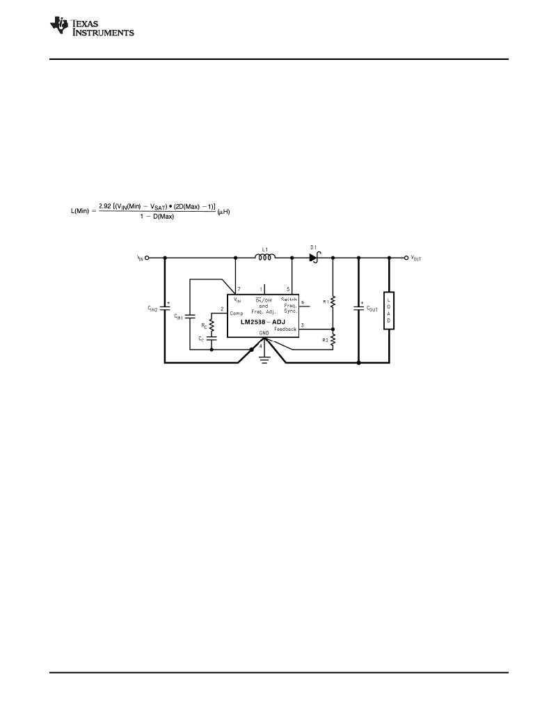
�STABILITY�
�All� current-mode� controlled� regulators� can� suffer� from� an� instability,� known� as� subharmonic� oscillation,� if� they�
�operate� with� a� duty� cycle� above� 50%.� To� eliminate� subharmonic� oscillations,� a� minimum� value� of� inductance� is�
�required� to� ensure� stability� for� all� boost� and� flyback� regulators.� The� minimum� inductance� is� given� by:�
�(6)�
�where� V� SAT� is� the� switch� saturation� voltage� and� can� be� found� in� the� Characteristic� Curves.�
�Figure� 60.� Circuit� Board� Layout�
�CIRCUIT� LAYOUT� GUIDELINES�
�As� in� any� switching� regulator,� layout� is� very� important.� Rapidly� switching� currents� associated� with� wiring�
�inductance� generate� voltage� transients� which� can� cause� problems.� For� minimal� inductance� and� ground� loops,�
�keep� the� length� of� the� leads� and� traces� as� short� as� possible.� Use� single� point� grounding� or� ground� plane�
�construction� for� best� results.� Separate� the� signal� grounds� from� the� power� grounds� (as� indicated� in� Figure� 60� ).�
�When� using� the� Adjustable� version,� physically� locate� the� programming� resistors� as� near� the� regulator� IC� as�
�possible,� to� keep� the� sensitive� feedback� wiring� short.�
�HEAT� SINK/THERMAL� CONSIDERATIONS�
�In� many� cases,� a� heat� sink� is� not� required� to� keep� the� LM2588� junction� temperature� within� the� allowed� operating�
�temperature� range.� For� each� application,� to� determine� whether� or� not� a� heat� sink� will� be� required,� the� following�
�must� be� identified:�
�1)� Maximum� ambient� temperature� (in� the� application).�
�2)� Maximum� regulator� power� dissipation� (in� the� application).�
�3)� Maximum� allowed� junction� temperature� (125°C� for� the� LM2588).� For� a� safe,� conservative� design,� a�
�temperature� approximately� 15°C� cooler� than� the� maximum� junction� temperature� should� be� selected� (110°C).�
�4)� LM2588� package� thermal� resistances� θ� JA� and� θ� JC� (given� in� the� Electrical� Characteristics).�
�Total� power� dissipated� (P� D� )� by� the� LM2588� can� be� estimated� as� follows:�
�Boost:�
�Copyright� ?� 1998–2013,� Texas� Instruments� Incorporated�
�Product� Folder� Links:� LM2588�
��29�
�相关PDF资料 |
PDF描述 |
|---|---|
| ZL2101ALAF | IC REG BUCK SYNC ADJ 6A 36QFN |
| LQP03TN2N2B02D | INDUCT 2.2NH+/-0.1NH 600MA 0201 |
| CDRH5D18-5R4NC | INDUCTOR 5.4UH SHIELDED SMD |
| GBM22DRMN-S273 | CONN EDGECARD 44POS .156 SQ WW |
| MAX16074RS25D1+T | IC MPU SUPERVISOR CIRCUIT 4UCSP |
相关代理商/技术参数 |
参数描述 |
|---|---|
| LM2588T-5.0 | 功能描述:直流/直流开关转换器 RoHS:否 制造商:STMicroelectronics 最大输入电压:4.5 V 开关频率:1.5 MHz 输出电压:4.6 V 输出电流:250 mA 输出端数量:2 最大工作温度:+ 85 C 安装风格:SMD/SMT |
| LM2588T-5.0/NOPB | 功能描述:直流/直流开关转换器 RoHS:否 制造商:STMicroelectronics 最大输入电压:4.5 V 开关频率:1.5 MHz 输出电压:4.6 V 输出电流:250 mA 输出端数量:2 最大工作温度:+ 85 C 安装风格:SMD/SMT |
| LM2588T50 | 制造商:Texas Instruments 功能描述:SWITCHING REG 5A 5.0V 2588 TO-220 |
| LM2588T-ADJ | 功能描述:直流/直流开关转换器 RoHS:否 制造商:STMicroelectronics 最大输入电压:4.5 V 开关频率:1.5 MHz 输出电压:4.6 V 输出电流:250 mA 输出端数量:2 最大工作温度:+ 85 C 安装风格:SMD/SMT |
| LM2588T-ADJ | 制造商:Texas Instruments 功能描述:SWITCHING REG 5A ADJ 2588 TO2207 |
发布紧急采购,3分钟左右您将得到回复。