- 您现在的位置:买卖IC网 > PDF目录17351 > LM2595ADPBCKGEVB (ON Semiconductor)EVAL BOARD FOR LM2595ADPBCKG PDF资料下载
参数资料
| 型号: | LM2595ADPBCKGEVB |
| 厂商: | ON Semiconductor |
| 文件页数: | 19/25页 |
| 文件大小: | 0K |
| 描述: | EVAL BOARD FOR LM2595ADPBCKG |
| 设计资源: | LM2595ADPBCKGEVB BOM LM2595ADPBCKGEVB Gerber Files LM2595ADPBCKGEVB Schematic |
| 标准包装: | 1 |
| 主要目的: | DC/DC,步降 |
| 输出及类型: | 1,非隔离 |
| 输出电压: | 5V |
| 电流 - 输出: | 1A |
| 输入电压: | 4.5 ~ 40 V |
| 稳压器拓扑结构: | 降压 |
| 频率 - 开关: | 150kHz |
| 板类型: | 完全填充 |
| 已供物品: | 板 |
| 已用 IC / 零件: | LM2595 |
| 其它名称: | LM2595ADPBCKGEVBOS |
�� �
�
�LM2595�
�+V� in�
�+V� in�
�7�
�LM2595�
�+V�
�0�
�On�
�Off�
�R2�
�Shutdown�
�Input�
�5.0� V�
�0�
�Off�
�On�
�Shutdown�
�Input�
�R3�
�470�
�C� in� R1�
�100� m� F� 47� k�
�5�
�ON/OFF� 6�
�R2�
�GN�
�D�
�+V� in�
�5.6� k�
�C� in�
�100� m� F�
�Q1�
�+V� in�
�7�
�LM2595�
�47� k�
�2N3906�
�5�
�ON/OFF� 6�
�GN�
�-V� out�
�D�
�MOC8101�
�R1�
�12� k�
�-V� out�
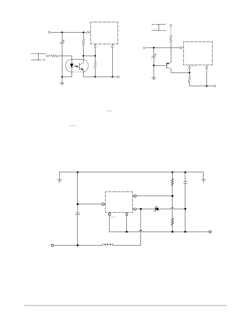
�NOTE:� This� picture� does� not� show� the� complete� circuit.�
�Figure� 25.� Inverting� Buck� ?� Boost� Regulator� Shutdown�
�Circuit� Using� an� Optocoupler�
�With� the� inverting� configuration,� the� use� of� the� ON/OFF�
�pin� requires� some� level� shifting� techniques.� This� is� caused�
�by� the� fact,� that� the� ground� pin� of� the� converter� IC� is� no�
�longer� at� ground.� Now,� the� ON/OFF� pin� threshold� voltage�
�(1.3� V� approximately)� has� to� be� related� to� the� negative�
�output� voltage� level.� There� are� many� different� possible� shut�
�down� methods,� two� of� them� are� shown� in� Figures� 25� and� 26.�
�NOTE:� This� picture� does� not� show� the� complete� circuit.�
�Figure� 26.� Inverting� Buck� ?� Boost� Regulator� Shutdown�
�Circuit� Using� a� PNP� Transistor�
�Negative� Boost� Regulator�
�This� example� is� a� variation� of� the� buck� ?� boost� topology�
�and� it� is� called� negative� boost� regulator.� This� regulator�
�experiences� relatively� high� switch� current,� especially� at� low�
�input� voltages.� The� internal� switch� current� limiting� results� in�
�lower� output� load� current� capability.�
�The� circuit� in� Figure� 27� shows� the� negative� boost�
�configuration.� The� input� voltage� in� this� application� ranges�
�from� ?� 5.0� V� to� ?� 12� V� and� provides� a� regulated� ?� 12� V� output.�
�If� the� input� voltage� is� greater� than� ?� 12� V,� the� output� will� rise�
�above� ?� 12� V� accordingly,� but� will� not� damage� the� regulator.�
�R4�
�Feedback�
�C� out�
�470� m� F�
�+V� in�
�LM2595�
�C� in�
�100� m� F/�
�50� V�
�ON/OFF�
�GND�
�D1�
�1N5822�
�R3�
�?� 12� V� @� 0.25� A�
�Regulated�
�Output�
�?� 12� V�
�Unregulated�
�DC� Input�
�L1�
�100� m� H�
�Figure� 27.� Negative� Boost� Regulator�
�Design� Recommendations:�
�The� same� design� rules� as� for� the� previous� inverting�
�buck� ?� boost� converter� can� be� applied.� The� output� capacitor�
�C� out� must� be� chosen� larger� than� would� be� required� for� a� what�
�standard� buck� converter.� Low� input� voltages� or� high� output�
�currents� require� a� large� value� output� capacitor� (in� the� range�
�of� thousands� of� m� F).� The� recommended� range� of� inductor�
�values� for� the� negative� boost� regulator� is� the� same� as� for�
�inverting� converter� design.�
�Another� important� point� is� that� these� negative� boost�
�converters� cannot� provide� current� limiting� load� protection� in�
�the� event� of� a� short� in� the� output� so� some� other� means,� such�
�as� a� fuse,� may� be� necessary� to� provide� the� load� protection.�
�http://onsemi.com�
�19�
�相关PDF资料 |
PDF描述 |
|---|---|
| R1S12-0505/P-R | CONV DC/DC 1W 05VIN 05VOUT |
| AS1329B EB | BOARD EVAL AS1329B |
| SJA7501-1-1/2-50-WHITE | LOOP WHITE 1 1/2" X 50YD 0.12" |
| ECM08DRYH | CONN EDGECARD 16POS DIP .156 SLD |
| CS51411EVB | EVAL BOARD FOR CS51411 HI FREQ |
相关代理商/技术参数 |
参数描述 |
|---|---|
| LM2595ATPBCKGEVB | 功能描述:电源管理IC开发工具 LM2595ADJ TO220 BUCK DB RoHS:否 制造商:Maxim Integrated 产品:Evaluation Kits 类型:Battery Management 工具用于评估:MAX17710GB 输入电压: 输出电压:1.8 V |
| LM2595DSADJG | 功能描述:直流/直流开关调节器 1A BUCK SW REG 150KHZ RoHS:否 制造商:International Rectifier 最大输入电压:21 V 开关频率:1.5 MHz 输出电压:0.5 V to 0.86 V 输出电流:4 A 输出端数量: 最大工作温度: 安装风格:SMD/SMT 封装 / 箱体:PQFN 4 x 5 |
| LM2595DSADJR4G | 功能描述:直流/直流开关调节器 1A BUCK SW REG 150KHZ RoHS:否 制造商:International Rectifier 最大输入电压:21 V 开关频率:1.5 MHz 输出电压:0.5 V to 0.86 V 输出电流:4 A 输出端数量: 最大工作温度: 安装风格:SMD/SMT 封装 / 箱体:PQFN 4 x 5 |
| LM2595S12 | 制造商:Texas Instruments 功能描述:SWITCHING REG, 1A 12V, SMD, 2595 制造商:Texas Instruments 功能描述:SWITCHING REG, 1A 12V, SMD, 2595; Primary Input Voltage:24V; No. of Outputs:1; Output Voltage:12V; Output Current:1A; Voltage Regulator Case Style:TO-263; No. of Pins:5; Operating Temperature Min:-25C; Operating Temperature ;RoHS Compliant: Yes |
| LM2595S-12 | 功能描述:直流/直流开关转换器 RoHS:否 制造商:STMicroelectronics 最大输入电压:4.5 V 开关频率:1.5 MHz 输出电压:4.6 V 输出电流:250 mA 输出端数量:2 最大工作温度:+ 85 C 安装风格:SMD/SMT |
发布紧急采购,3分钟左右您将得到回复。