- 您现在的位置:买卖IC网 > PDF目录44549 > LM2599-5.0MWC (NATIONAL SEMICONDUCTOR CORP) 7.5 A SWITCHING REGULATOR, 173 kHz SWITCHING FREQ-MAX, UUC PDF资料下载
参数资料
| 型号: | LM2599-5.0MWC |
| 厂商: | NATIONAL SEMICONDUCTOR CORP |
| 元件分类: | 稳压器 |
| 英文描述: | 7.5 A SWITCHING REGULATOR, 173 kHz SWITCHING FREQ-MAX, UUC |
| 封装: | WAFER |
| 文件页数: | 17/36页 |
| 文件大小: | 897K |
| 代理商: | LM2599-5.0MWC |
第1页第2页第3页第4页第5页第6页第7页第8页第9页第10页第11页第12页第13页第14页第15页第16页当前第17页第18页第19页第20页第21页第22页第23页第24页第25页第26页第27页第28页第29页第30页第31页第32页第33页第34页第35页第36页
Application Information (Continued)
determining a number of other circuit parameters. Param-
eters such as, peak inductor or peak switch current, mini-
mum load current before the circuit becomes discontinuous,
output ripple voltage and output capacitor ESR can all be
calculated from the peak-to-peak
I
IND. When the inductor
nomographs shown in
Figure 4 through 7 are used to select
an inductor value, the peak-to-peak inductor ripple current
can immediately be determined. The curve shown in
Figure
21 shows the range of (
I
IND) that can be expected for
different load currents. The curve also shows how the
peak-to-peak inductor ripple current (
I
IND) changes as you
go from the lower border to the upper border (for a given load
current) within an inductance region. The upper border rep-
resents a higher input voltage, while the lower border repre-
sents a lower input voltage (see Inductor Selection Guides).
These curves are only correct for continuous mode opera-
tion, and only if the inductor selection guides are used to
select the inductor value
Consider the following example:
V
OUT = 5V, maximum load current of 2.5A
V
IN = 12V, nominal, varying between 10V and 16V.
The selection guide in
Figure 5 shows that the vertical line
for a 2.5A load current, and the horizontal line for the 12V
input voltage intersect approximately midway between the
upper and lower borders of the 33 H inductance region. A
33 H inductor will allow a peak-to-peak inductor current
(
I
IND) to flow that will be a percentage of the maximum load
current. Referring to
Figure 21, follow the 2.5A line approxi-
mately midway into the inductance region, and read the
peak-to-peak inductor ripple current (
I
IND) on the left hand
axis (approximately 620 mA p-p).
As the input voltage increases to 16V, it approaches the
upper border of the inductance region, and the inductor
ripple current increases. Referring to the curve in
Figure 21,
it can be seen that for a load current of 2.5A, the
peak-to-peak inductor ripple current (
I
IND) is 620 mA with
12V in, and can range from 740 mA at the upper border (16V
in) to 500 mA at the lower border (10V in).
Once the
I
IND value is known, the following formulas can be
used to calculate additional information about the switching
regulator circuit.
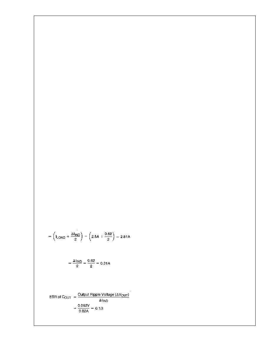
1.
Peak Inductor or peak switch current
2.
Minimum load current before the circuit becomes dis-
continuous
3.
Output Ripple Voltage = (
I
IND)x(ESR of COUT)
= 0.62Ax0.1
=62mVp-p
4.
OPEN CORE INDUCTORS
Another possible source of increased output ripple voltage or
unstable operation is from an open core inductor. Ferrite
bobbin or stick inductors have magnetic lines of flux flowing
through the air from one end of the bobbin to the other end.
These magnetic lines of flux will induce a voltage into any
wire or PC board copper trace that comes within the induc-
tor’s magnetic field. The strength of the magnetic field, the
orientation and location of the PC copper trace to the mag-
netic field, and the distance between the copper trace and
the inductor, determine the amount of voltage generated in
the copper trace. Another way of looking at this inductive
coupling is to consider the PC board copper trace as one
turn of a transformer (secondary) with the inductor winding
as the primary. Many millivolts can be generated in a copper
trace located near an open core inductor which can cause
stability problems or high output ripple voltage problems.
If unstable operation is seen, and an open core inductor is
used, it’s possible that the location of the inductor with
respect to other PC traces may be the problem. To deter-
mine if this is the problem, temporarily raise the inductor
away from the board by several inches and then check
circuit operation. If the circuit now operates correctly, then
the magnetic flux from the open core inductor is causing the
problem. Substituting a closed core inductor such as a tor-
roid or E-core will correct the problem, or re-arranging the
PC layout may be necessary. Magnetic flux cutting the IC
device ground trace, feedback trace, or the positive or nega-
tive traces of the output capacitor should be minimized.
Sometimes, locating a trace directly beneath a bobbin in-
ductor will provide good results, provided it is exactly in the
center of the inductor (because the induced voltages cancel
themselves out), but if it is off center one direction or the
other, then problems could arise. If flux problems are
present, even the direction of the inductor winding can make
a difference in some circuits.
This discussion on open core inductors is not to frighten the
user, but to alert the user on what kind of problems to watch
out for when using them. Open core bobbin or “stick” induc-
tors are an inexpensive, simple way of making a compact
efficient inductor, and they are used by the millions in many
different applications.
THERMAL CONSIDERATIONS
The LM2599 is available in two packages, a 7-pin TO-220
(T) and a 7-pin surface mount TO-263 (S).
The TO-220 package needs a heat sink under most condi-
tions. The size of the heat sink depends on the input voltage,
the output voltage, the load current and the ambient tem-
perature. The curves in
Figure 22 show the LM2599T junc-
tion temperature rises above ambient temperature for a 3A
load and different input and output voltages. The data for
these curves was taken with the LM2599T (TO-220 pack-
age) operating as a buck switching regulator in an ambient
temperature of 25C (still air). These temperature rise num-
bers are all approximate and there are many factors that can
affect these temperatures. Higher ambient temperatures re-
quire more heat sinking.
The TO-263 surface mount package tab is designed to be
soldered to the copper on a printed circuit board. The copper
and the board are the heat sink for this package and the
other heat producing components, such as the catch diode
and inductor. The pc board copper area that the package is
soldered to should be at least 0.4 in2, and ideally should
have 2 or more square inches of 2 oz. (0.0028 in) copper.
Additional copper area improves the thermal characteristics,
LM2599
www.national.com
24
相关PDF资料 |
PDF描述 |
|---|---|
| LM2599-3.3MDC | 7.5 A SWITCHING REGULATOR, 173 kHz SWITCHING FREQ-MAX, UUC |
| LM2599-ADJMWC | 7.5 A SWITCHING REGULATOR, 173 kHz SWITCHING FREQ-MAX, UUC |
| LM2599-3.3MWC | 7.5 A SWITCHING REGULATOR, 173 kHz SWITCHING FREQ-MAX, UUC |
| LM2621MDC | 2.85 A SWITCHING REGULATOR, 2000 kHz SWITCHING FREQ-MAX, UUC |
| LM2622-ADJMWC | 2.3 A SWITCHING REGULATOR, 1500 kHz SWITCHING FREQ-MAX, UUC |
相关代理商/技术参数 |
参数描述 |
|---|---|
| LM2599S-12 | 功能描述:直流/直流开关转换器 RoHS:否 制造商:STMicroelectronics 最大输入电压:4.5 V 开关频率:1.5 MHz 输出电压:4.6 V 输出电流:250 mA 输出端数量:2 最大工作温度:+ 85 C 安装风格:SMD/SMT |
| LM2599S-12/NOPB | 功能描述:直流/直流开关转换器 RoHS:否 制造商:STMicroelectronics 最大输入电压:4.5 V 开关频率:1.5 MHz 输出电压:4.6 V 输出电流:250 mA 输出端数量:2 最大工作温度:+ 85 C 安装风格:SMD/SMT |
| LM2599S-3.3 | 功能描述:直流/直流开关转换器 RoHS:否 制造商:STMicroelectronics 最大输入电压:4.5 V 开关频率:1.5 MHz 输出电压:4.6 V 输出电流:250 mA 输出端数量:2 最大工作温度:+ 85 C 安装风格:SMD/SMT |
| LM2599S-3.3/NOPB | 功能描述:直流/直流开关转换器 RoHS:否 制造商:STMicroelectronics 最大输入电压:4.5 V 开关频率:1.5 MHz 输出电压:4.6 V 输出电流:250 mA 输出端数量:2 最大工作温度:+ 85 C 安装风格:SMD/SMT |
| LM2599S-5.0 | 功能描述:直流/直流开关转换器 RoHS:否 制造商:STMicroelectronics 最大输入电压:4.5 V 开关频率:1.5 MHz 输出电压:4.6 V 输出电流:250 mA 输出端数量:2 最大工作温度:+ 85 C 安装风格:SMD/SMT |
发布紧急采购,3分钟左右您将得到回复。