- 您现在的位置:买卖IC网 > PDF目录44549 > LM2622-ADJMWC (NATIONAL SEMICONDUCTOR CORP) 2.3 A SWITCHING REGULATOR, 1500 kHz SWITCHING FREQ-MAX, UUC PDF资料下载
参数资料
| 型号: | LM2622-ADJMWC |
| 厂商: | NATIONAL SEMICONDUCTOR CORP |
| 元件分类: | 稳压器 |
| 英文描述: | 2.3 A SWITCHING REGULATOR, 1500 kHz SWITCHING FREQ-MAX, UUC |
| 封装: | WAFER |
| 文件页数: | 15/19页 |
| 文件大小: | 478K |
| 代理商: | LM2622-ADJMWC |
Electrical Characteristics (Continued)
Note 3: The human body model is a 100 pF capacitor discharged through a 1.5k
resistor into each pin. The machine model is a 200pF capacitor discharged
directly into each pin.
Note 4: All limits guaranteed at room temperature (standard typeface) and at temperature extremes (bold typeface). All room temperature limits are 100%
production tested. All limits at temperature extremes are guaranteed via correlation using standard Statistical Quality Control (SQC) methods. All limits are used to
calculate Average Outgoing Quality Level (AOQL).
Note 5: Typical numbers are at 25C and represent the most likely norm.
Note 6: Duty cycle affects current limit due to ramp generator.
Note 7: Current limit at 0% duty cycle. See TYPICAL PERFORMANCE section for Switch Current Limit vs. VIN
Note 8: Bias current flows into FB pin.
Note 9: Junction to ambient thermal resistance (no external heat sink) for the MSO8 package with minimal trace widths (0.010 inches) from the pins to the circuit.
See ’Scenario ’A’’ in the Power Dissipation section.
Note 10: Junction to ambient thermal resistance for the MSO8 package with minimal trace widths (0.010 inches) from the pins to the circuit and approximately
0.0191 sq. in. of copper heat sinking. See ’Scenario ’B’’ in the Power Dissipation section.
Note 11: Junction to ambient thermal resistance for the MSO8 package with minimal trace widths (0.010 inches) from the pins to the circuit and approximately
0.0465 sq. in. of copper heat sinking. See ’Scenario ’C’’ in the Power Dissipation section.
Note 12: Junction to ambient thermal resistance for the MSO8 package with minimal trace widths (0.010 inches) from the pins to the circuit and approximately
0.2523 sq. in. of copper heat sinking. See ’Scenario ’D’’ in the Power Dissipation section.
Note 13: Junction to ambient thermal resistance for the MSO8 package with minimal trace widths (0.010 inches) from the pins to the circuit and approximately
0.0098 sq. in. of copper heat sinking on the top layer and 0.0760 sq. in. of copper heat sinking on the bottom layer, with three 0.020 in. vias connecting the planes.
See ’Scenario ’E’’ in the Power Dissipation section.
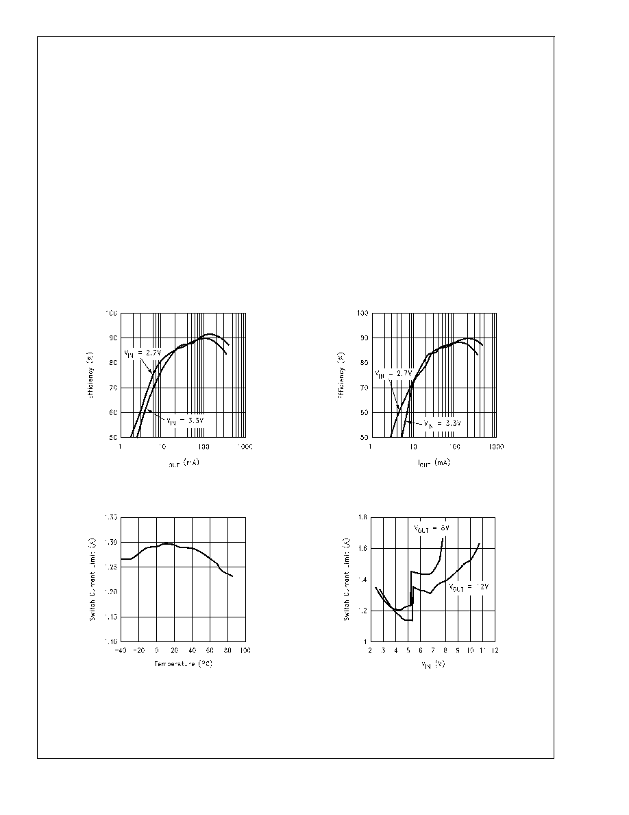
Typical Performance Characteristics
Efficiency vs. Load Current
(V
OUT = 8V, fS = 600 kHz)
Efficiency vs. Load Current
(V
OUT = 8V, fS = 1.3 MHz)
10127326
10127325
Switch Current Limit vs. Temperature
(V
IN = 3.3V, VOUT = 8V)
Switch Current Limit vs. V
IN
10127320
10127322
LM2622
www.national.com
5
相关PDF资料 |
PDF描述 |
|---|---|
| LM2630MTC-ADJ/NOPB | SWITCHING CONTROLLER, 345 kHz SWITCHING FREQ-MAX, PDSO20 |
| LM2630MTC-ADJX | SWITCHING CONTROLLER, 345 kHz SWITCHING FREQ-MAX, PDSO20 |
| LM2631MTCX-ADJ/NOPB | SWITCHING CONTROLLER, 400 kHz SWITCHING FREQ-MAX, PDSO20 |
| LM2636MWC | SWITCHING CONTROLLER, 2000 kHz SWITCHING FREQ-MAX, UUC |
| LM2636MX/NOPB | SWITCHING CONTROLLER, 2000 kHz SWITCHING FREQ-MAX, PDSO20 |
相关代理商/技术参数 |
参数描述 |
|---|---|
| LM2622EVAL | 功能描述:BOARD EVALUATION LM2622 RoHS:否 类别:编程器,开发系统 >> 评估板 - DC/DC 与 AC/DC(离线)SMPS 系列:- 产品培训模块:Obsolescence Mitigation Program 标准包装:1 系列:True Shutdown™ 主要目的:DC/DC,步升 输出及类型:1,非隔离 功率 - 输出:- 输出电压:- 电流 - 输出:1A 输入电压:2.5 V ~ 5.5 V 稳压器拓扑结构:升压 频率 - 开关:3MHz 板类型:完全填充 已供物品:板 已用 IC / 零件:MAX8969 |
| LM2622MM-ADJ | 功能描述:DC/DC 开关控制器 RoHS:否 制造商:Texas Instruments 输入电压:6 V to 100 V 开关频率: 输出电压:1.215 V to 80 V 输出电流:3.5 A 输出端数量:1 最大工作温度:+ 125 C 安装风格: 封装 / 箱体:CPAK |
| LM2622MM-ADJ/NOPB | 功能描述:DC/DC 开关控制器 RoHS:否 制造商:Texas Instruments 输入电压:6 V to 100 V 开关频率: 输出电压:1.215 V to 80 V 输出电流:3.5 A 输出端数量:1 最大工作温度:+ 125 C 安装风格: 封装 / 箱体:CPAK |
| LM2622MMX-ADJ | 制造商:Texas Instruments 功能描述:Conv DC-DC Single Step Up 2V to 12V 8-Pin MSOP T/R |
| LM2622MMX-ADJ/NOPB | 功能描述:DC/DC 开关控制器 RoHS:否 制造商:Texas Instruments 输入电压:6 V to 100 V 开关频率: 输出电压:1.215 V to 80 V 输出电流:3.5 A 输出端数量:1 最大工作温度:+ 125 C 安装风格: 封装 / 箱体:CPAK |
发布紧急采购,3分钟左右您将得到回复。