- 您现在的位置:买卖IC网 > PDF目录39246 > LM2636M/NOPB (NATIONAL SEMICONDUCTOR CORP) SWITCHING CONTROLLER, 2000 kHz SWITCHING FREQ-MAX, PDSO20 PDF资料下载
参数资料
| 型号: | LM2636M/NOPB |
| 厂商: | NATIONAL SEMICONDUCTOR CORP |
| 元件分类: | 稳压器 |
| 英文描述: | SWITCHING CONTROLLER, 2000 kHz SWITCHING FREQ-MAX, PDSO20 |
| 封装: | PLASTIC, SO-20 |
| 文件页数: | 8/15页 |
| 文件大小: | 766K |
| 代理商: | LM2636M/NOPB |
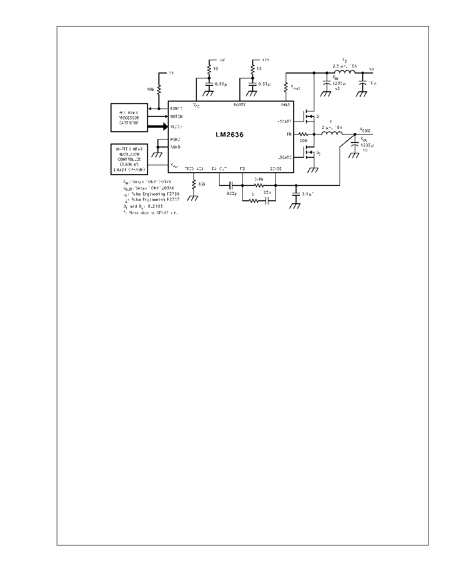
Typical Application
Pin Descriptions
LSGATE (Pin 1): Gate drive for the low-side N-channel
MOSFET. This signal is interlocked with HSGATE (Pin 20) to
avoid a shoot-through problem.
BOOTV (Pin 2): Power supply for high-side N-channel
MOSFET gate drive. The voltage should be at least one gate
threshold above the converter input voltage to properly op-
erate the high-side N-FET.
PGND (Pin 3): Ground for high current circuitry. It should be
connected to system ground.
SGND (Pin 4): Ground for signal level circuitry. It should be
connected to system ground.
V
CC (Pin 5): Power supply for the controller.
SENSE (Pin 6): Converter output voltage sensing. It pro-
vides input for power good, fast dual comparator control
loop, and over-voltage protection circuitry. It is recom-
mended that a 0.1 F capacitor be connected between this
pin and ground to avoid potential noise problems.
IMAX (Pin 7): Current limit threshold setting. It sinks a fixed
180 A current. By connecting a resistor between the high
side MOSFET drain and this pin, a fixed voltage drop can be
built across the resistor. This voltage drop is compared with
the V
DS of the high-side N-MOSFET to determine if an
over-current condition has occurred.
IFB (Pin 8): High-side N-MOSFET source voltage sensing.
This pin is one V
DS below drain voltage. When this voltage is
lower than that of IMAX pin during the time the high-side FET
is on, it means V
DS is higher than the preset voltage across
the IMAX resistor, which can be interpreted as an over-
current condition.
V
REF (Pin 9): Bandgap reference voltage. This voltage is
mainly for use by other power supplies on the motherboard
which need a reference.
EA_OUT (Pin 10): Output of the error amplifier. The voltage
level on this pin is compared with an internally generated
ramp signal to determine the duty cycle. This pin is neces-
sary for compensating the primary control loop.
FB (Pin 11): Inverting input of the error amplifier. A pin
necessary for compensating the control loop.
FREQ_ADJ (Pin 12): Switching frequency adjustment.
Switching frequency can be adjusted by changing the
grounding resistance on this pin.
PWRGD (Pin 13): Power Good. There are two windows
around the DAC output voltage that are associated with
PWRGD pin, the ±10% window and the ±8% window. If
PWRGD is initially high (open drain state) and output voltage
travels out of ±10% window, PWRGD goes to low (low
impedance to ground). If PWRGD is initially low and output
voltage travels into the ±8% window and has stayed within
the window for at least 10 ms, PWRGD goes to high. A
PWRGD high means the output voltage is at least within the
±10% window whereas a PWRGD low indicates the output
voltage is definitely outside the ±8% window.
VID4:0 (Pins 14, 15, 16, 17, 18): Voltage Identification
Code. The five pins accept an open-ground pattern 5-bit
binary code from outside the chip (typically from the CPU) for
generating the desired output voltage. Each VID pin is inter-
nally pulled up to V
CC via a 90 A current source. Table 1
shows the code table.
OUTEN (Pin 19): Output Enable. The output voltage is
disabled when this pin is pulled low. It is internally pulled up
to V
CC via a 90 A current source.
HSGATE (Pin 20): Gate drive for the high-side N-channel
MOSFET. This signal is interlocked with LSGATE (Pin 1) to
avoid a shoot-through problem.
10083401
FIGURE 1. 5V to 1.3V–3.5V, 14A Power Supply
LM2636
www.national.com
2
相关PDF资料 |
PDF描述 |
|---|---|
| LM2661MDC | SWITCHED CAPACITOR CONVERTER, 80 kHz SWITCHING FREQ-MAX, UUC |
| LM2675-5.0MDC | 2.2 A SWITCHING REGULATOR, 275 kHz SWITCHING FREQ-MAX, UUC |
| LM2675-5.0MWC | 2.2 A SWITCHING REGULATOR, 275 kHz SWITCHING FREQ-MAX, UUC |
| LM2675-12MWC | 2.2 A SWITCHING REGULATOR, 275 kHz SWITCHING FREQ-MAX, UUC |
| LM2682MX/NOPB | SWITCHED CAPACITOR CONVERTER, 15 kHz SWITCHING FREQ-MAX, PDSO8 |
相关代理商/技术参数 |
参数描述 |
|---|---|
| LM2636MTC | 制造商:OC White Company 功能描述:DC DC Cntrlr Single-OUT Sync Buck 4.5V to 5.5V Input 20-Pin TSSOP Rail |
| LM2636MTC/NOPB | 功能描述:IC REG SYNCH BUCK 5-BIT 20-TSSOP RoHS:是 类别:集成电路 (IC) >> PMIC - 电源管理 - 专用 系列:- 应用说明:Ultrasound Imaging Systems Application Note 产品培训模块:Lead (SnPb) Finish for COTS Obsolescence Mitigation Program 标准包装:37 系列:- 应用:医疗用超声波成像,声纳 电流 - 电源:- 电源电压:2.37 V ~ 6 V 工作温度:0°C ~ 70°C 安装类型:表面贴装 封装/外壳:56-WFQFN 裸露焊盘 供应商设备封装:56-TQFN-EP(8x8) 包装:管件 |
| LM2636MTCX | 制造商:未知厂家 制造商全称:未知厂家 功能描述:Voltage-Mode SMPS Controller |
| LM2636MTCX/NOPB | 功能描述:IC CTRLR PROG REG 5BIT 20TSSOP RoHS:是 类别:集成电路 (IC) >> PMIC - 电源管理 - 专用 系列:- 应用说明:Ultrasound Imaging Systems Application Note 产品培训模块:Lead (SnPb) Finish for COTS Obsolescence Mitigation Program 标准包装:37 系列:- 应用:医疗用超声波成像,声纳 电流 - 电源:- 电源电压:2.37 V ~ 6 V 工作温度:0°C ~ 70°C 安装类型:表面贴装 封装/外壳:56-WFQFN 裸露焊盘 供应商设备封装:56-TQFN-EP(8x8) 包装:管件 |
| LM2636MX | 制造商:Texas Instruments 功能描述: |
发布紧急采购,3分钟左右您将得到回复。