- 您现在的位置:买卖IC网 > PDF目录39246 > LM2636MTC/NOPB (NATIONAL SEMICONDUCTOR CORP) SWITCHING CONTROLLER, 2000 kHz SWITCHING FREQ-MAX, PDSO20 PDF资料下载
参数资料
| 型号: | LM2636MTC/NOPB |
| 厂商: | NATIONAL SEMICONDUCTOR CORP |
| 元件分类: | 稳压器 |
| 英文描述: | SWITCHING CONTROLLER, 2000 kHz SWITCHING FREQ-MAX, PDSO20 |
| 封装: | PLASTIC, TSSOP-20 |
| 文件页数: | 14/15页 |
| 文件大小: | 766K |
| 代理商: | LM2636MTC/NOPB |
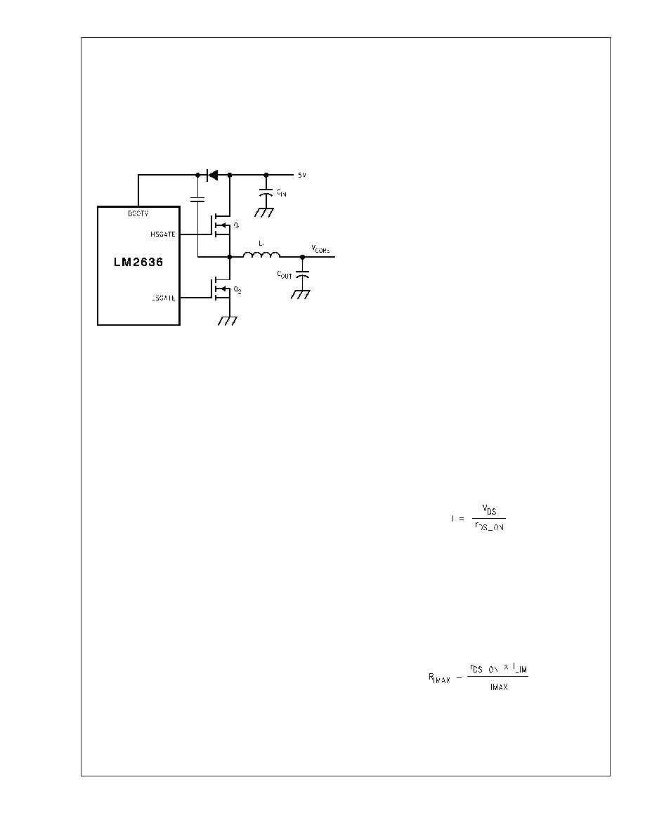
Applications Information (Continued)
fully turned on. The voltage can be either supplied from
a separate source other than the input voltage or can be
generated locally by utilizing a charge pump structure. In a
typical desktop microprocessor application, if 5V is chosen
to be the input voltage, then 12V can be used for the
BOOTV. If 12V is not available, a simple charge pump
circuitry consisting of a diode and a small capacitor can be
used, as shown in Figure 3.
When the low side FET is on, the charge pump capacitor is
charged to near the input voltage through the diode. When
low side FET is turned off, the high side FET driver is
enabled, and the charge pump capacitor starts to charge the
high side FET gate until it is fully on. By this time the high
side FET source node will fly to close to input voltage level
and the upper node of the capacitor will also fly to one input
voltage higher than the input voltage, enabling the high side
FET driver to continue working.
For a BOOTV of 12V, the initial gate charging current is
typically 2A, and the initial gate discharging current is typi-
cally 6A, good for high speed switching.
The LM2636 gate drives are of BiCMOS design. Unlike
some other bipolar VRM control ICs, the gate drive has
rail-to-rail swing that ensures no spurious turn-on due to
capacitive coupling.
Another feature of the FET gate drives is the adaptive non-
overlapping mechanism. A gate driver is not turned on until
the other is fully off. The dead time in between is typically 20
ns. This avoids the potential shoot-through problem and
helps improve efficiency.
Load Transient Response
In a typical modern MPU application such as the Pentium II
core voltage power supply, load transient response is a
critical issue. The LM2636 utilizes the conventional voltage
feedback technology as the primary feedback control
method. When the load transient happens, the error in the
output voltage level is fed to the error amplifier. The output of
the
error
amplifier
is
then
compared
with
an
internally generated PWM ramp signal and the result of the
comparison is a series of pulses with certain duty ratios.
These pulses are used to control the turn-on and turn-off of
the MOSFET gate drivers. In this way, the error in the output
voltage gets “compensated” or cancelled by the change in
the duty ratio of the FET switches. During a large load
transient, depending on the compensation design, the
change in duty ratio can be as fast as less than one switch-
ing cycle. Refer to Design Considerations section for more
details.
Besides the usual voltage mode feedback control loop, the
LM2636 also has a pair of fast comparators (the MIN and
MAX comparators) to help maintain the output voltage dur-
ing a large and fast load transient. The trip points of the
comparators are set to ±5% of the DAC output voltage.
When the load transient is so large that the output voltage
goes outside the ±5% window, the MIN or MAX comparator
will bypass the primary voltage control loop and immediately
set the duty ratio to either maximum value or to zero. This
provides the fastest possible way to react to such a large
load transient in a classical buck converter.
Power Good Signal
The power good signal is used to indicate that the output
voltage is within specified range. In the LM2636, the range is
set to a ±10% window of the DAC output voltage. During soft
start, the power good signal is always low. At the end of the
soft start session,the output voltage is checked and the
PWRGD pin will be asserted if the voltage is within specified
range.
Over Voltage Protection
When the output voltage exceeds 115% of the DAC output
voltage after the end of soft start, the LM2636 will enter over
voltage protection mode in which it shuts itself down. The
upper gate driver is held low while the lower gate driver is
held high. PWRGD will be low. For LM2636 to recover from
OVP mode, either OUTEN or V
CC voltage has to be toggled.
Another more subtle way to recover is to float all the VID pins
and reapply the correct code.
Current Limit
Current limit is realized by sensing the V
DS voltage of the
high side MOSFET when it is on. Since the r
DS_ON of a
MOSFET is a known value, current through the MOSFET
can be known by monitoring V
DS. The relationship between
the three parameters is:
To implement the current limit function, an external resistor
R
IMAX is need. The resistor should be connected between
the drain of the high side MOSFET and the IMAX pin. A
constant current of around 180 A is forced into the IMAX pin
and causes a fixed voltage drop across the R
IMAX resistor.
This voltage drop is then compared with the V
DS of the high
side MOSFET and if the latter is higher, over current is
reached. So the appropriate value of R
IMAX
for a pre-
determined current limit level I
LIM can be calculated by the
following equation:
For example, if we know that the r
DS_ON of the MOSFET is
20 m
, and the current limit we want to set is 20A, then we
should choose the value of R
IMAX to be 2.2 k
.
To provide the greatest protection over the high side MOS-
FET, cycle by cycle protection is implemented. The sampling
of the V
DS starts as early as about 300 ns after the switch is
10083406
FIGURE 3. BOOTV Voltage Supplied by a Charge Pump
LM2636
www.national.com
8
相关PDF资料 |
PDF描述 |
|---|---|
| LM2636M/NOPB | SWITCHING CONTROLLER, 2000 kHz SWITCHING FREQ-MAX, PDSO20 |
| LM2661MDC | SWITCHED CAPACITOR CONVERTER, 80 kHz SWITCHING FREQ-MAX, UUC |
| LM2675-5.0MDC | 2.2 A SWITCHING REGULATOR, 275 kHz SWITCHING FREQ-MAX, UUC |
| LM2675-5.0MWC | 2.2 A SWITCHING REGULATOR, 275 kHz SWITCHING FREQ-MAX, UUC |
| LM2675-12MWC | 2.2 A SWITCHING REGULATOR, 275 kHz SWITCHING FREQ-MAX, UUC |
相关代理商/技术参数 |
参数描述 |
|---|---|
| LM2636MTCX | 制造商:未知厂家 制造商全称:未知厂家 功能描述:Voltage-Mode SMPS Controller |
| LM2636MTCX/NOPB | 功能描述:IC CTRLR PROG REG 5BIT 20TSSOP RoHS:是 类别:集成电路 (IC) >> PMIC - 电源管理 - 专用 系列:- 应用说明:Ultrasound Imaging Systems Application Note 产品培训模块:Lead (SnPb) Finish for COTS Obsolescence Mitigation Program 标准包装:37 系列:- 应用:医疗用超声波成像,声纳 电流 - 电源:- 电源电压:2.37 V ~ 6 V 工作温度:0°C ~ 70°C 安装类型:表面贴装 封装/外壳:56-WFQFN 裸露焊盘 供应商设备封装:56-TQFN-EP(8x8) 包装:管件 |
| LM2636MX | 制造商:Texas Instruments 功能描述: |
| LM2636MX/NOPB | 功能描述:IC CTRLR PROG REG 5BIT 20-SOIC RoHS:是 类别:集成电路 (IC) >> PMIC - 电源管理 - 专用 系列:- 应用说明:Ultrasound Imaging Systems Application Note 产品培训模块:Lead (SnPb) Finish for COTS Obsolescence Mitigation Program 标准包装:37 系列:- 应用:医疗用超声波成像,声纳 电流 - 电源:- 电源电压:2.37 V ~ 6 V 工作温度:0°C ~ 70°C 安装类型:表面贴装 封装/外壳:56-WFQFN 裸露焊盘 供应商设备封装:56-TQFN-EP(8x8) 包装:管件 |
| LM2637 | 制造商:未知厂家 制造商全称:未知厂家 功能描述: |
发布紧急采购,3分钟左右您将得到回复。