- 您现在的位置:买卖IC网 > PDF目录44549 > LM2636MWC (NATIONAL SEMICONDUCTOR CORP) SWITCHING CONTROLLER, 2000 kHz SWITCHING FREQ-MAX, UUC PDF资料下载
参数资料
| 型号: | LM2636MWC |
| 厂商: | NATIONAL SEMICONDUCTOR CORP |
| 元件分类: | 稳压器 |
| 英文描述: | SWITCHING CONTROLLER, 2000 kHz SWITCHING FREQ-MAX, UUC |
| 封装: | WAFER |
| 文件页数: | 13/17页 |
| 文件大小: | 372K |
| 代理商: | LM2636MWC |
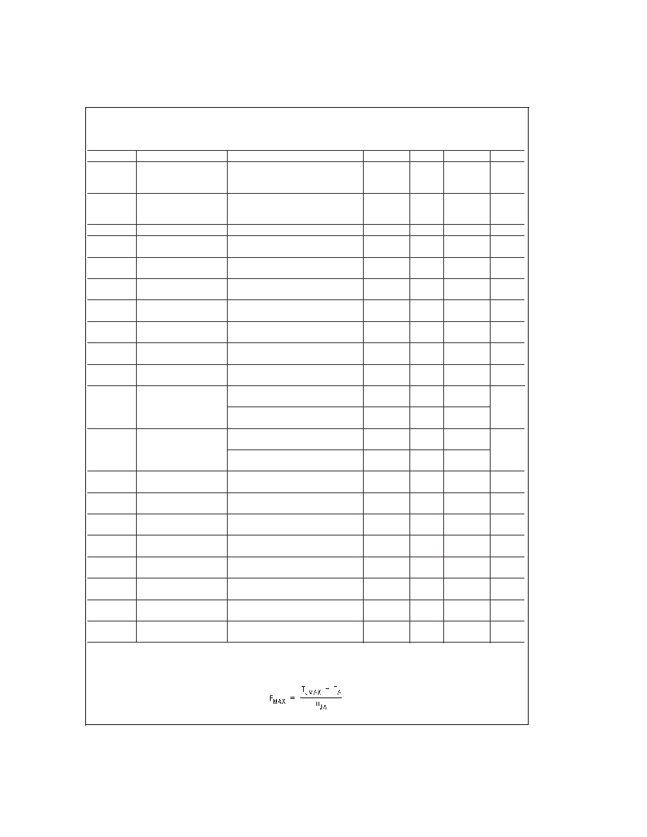
Electrical Characteristics (Continued)
V
CC = 5V unless otherwise indicated under the Conditions column. Typicals and limits appearing in plain type apply for TA =
T
J = +25C. Limits appearing in boldface type apply over 0C to +70C.
Symbol
Parameter
Conditions
Min
Typ
Max
Units
V
OUTEN_IH
OUTEN Pin Input Logic
Low to Logic High Trip
Point
OUTEN Voltage
↑
3.5
3.0
V
OUTEN_IL
OUTEN Pin Input Logic
High to Logic Low Trip
Point
OUTEN Voltage
↓
1.8
1.5
V
REF
Band Gap Reference
I
VREF =0mA
1.225
1.256
1.287
V
REF_LOAD
Reference Voltage at
Full Load
I
VREF = 0.5 mA, Sourcing
1.223
1.254
1.285
V
REF_525
Reference Voltage at
High Line
I
VREF = 0 mA, VCC = 5.25V
1.226
1.257
1.288
V
REF_475
Reference Voltage at
Low Line
I
VREF = 0 mA, VCC = 4.75V
1.224
1.255
1.286
V
REF_LOAD
Reference Voltage
Load Regulation
I
VREF = 0.5 mA, Sourcing
2
mV
V
REF_LINE
Reference Voltage Line
Regulation
I
VREF = 0 mA, VCC Changes from
5.25V to 4.75V
0.5
mV
V
SAWL
Ramp Signal Valley
Voltage
1.25
V
SAWH
Ramp Signal Peak
Voltage
3.25
V
PWRBAD_GD
PWRGD Pin
↓ Trip
Points (see Pin
Description for Pin 13)
% above DAC Output Voltage, when
Output Voltage
↑
10
%
% below DAC Output Voltage, when
Output Voltage
↓
10
V
PWRGD_BAD
PWRGD Pin
↑ Trip
Points (see Pin
Description for Pin 13)
% above DAC Output Voltage, when
Output Voltage
↓
8
%
% below DAC Output Voltage, when
Output Voltage
↑
8
V
OVP
Over-voltage Protection
Trip Point
% above DAC Output Voltage
15
%
t
PWRGD
Power Good Response
Time
V
SENSE Rises from 0V to Rated
V
OUT
2
6
15
s
t
PWRBAD
Power Not Good
Response Time
V
SENSE Falls from Rated VOUT to 0V
2
6
15
s
I
OUTEN
OUTEN Pin Internal
Pull-Up Current
60
90
130
A
V
VID_IH
VID Pins Logic High
Trip Point
3.5
3.0
V
VID_IL
VID Pins Logic Low
Trip Point
1.8
1.3
V
I
VID
VID0:4 Internal Pull-Up
Current
60
90
130
A
t
SS
Soft Start Duration
2048
clock
cycles
Note 1: Absolute Maximum Ratings are limits beyond which damage to the device may occur. Recommended Operating Conditions are conditions under which
the device operates correctly. Recommended Operating Conditions do not imply guaranteed performance limits.
Note 2: Maximum allowable DC power dissipation is a function of the maximum junction temperature, TJMAX , the junction-to-ambient thermal resistance, θJA, and
the ambient temperature, TA. The maximum allowable power dissipation at any ambient temperature is calculated using:
The junction-to-ambient thermal resistance,
θJA, for LM2636 in the M20B package is 88C/W, and 120C/W for the MTC20 package.
LM2636
www.national.com
5
相关PDF资料 |
PDF描述 |
|---|---|
| LM2636MX/NOPB | SWITCHING CONTROLLER, 2000 kHz SWITCHING FREQ-MAX, PDSO20 |
| LM2636MTCX/NOPB | SWITCHING CONTROLLER, 2000 kHz SWITCHING FREQ-MAX, PDSO20 |
| LM2637M/NOPB | SWITCHING CONTROLLER, 1000 kHz SWITCHING FREQ-MAX, PDSO24 |
| LM2637MWC | SWITCHING CONTROLLER, 1000 kHz SWITCHING FREQ-MAX, UUC |
| LM2639MX/NOPB | SWITCHING CONTROLLER, 8700 kHz SWITCHING FREQ-MAX, PDSO24 |
相关代理商/技术参数 |
参数描述 |
|---|---|
| LM2636MX | 制造商:Texas Instruments 功能描述: |
| LM2636MX/NOPB | 功能描述:IC CTRLR PROG REG 5BIT 20-SOIC RoHS:是 类别:集成电路 (IC) >> PMIC - 电源管理 - 专用 系列:- 应用说明:Ultrasound Imaging Systems Application Note 产品培训模块:Lead (SnPb) Finish for COTS Obsolescence Mitigation Program 标准包装:37 系列:- 应用:医疗用超声波成像,声纳 电流 - 电源:- 电源电压:2.37 V ~ 6 V 工作温度:0°C ~ 70°C 安装类型:表面贴装 封装/外壳:56-WFQFN 裸露焊盘 供应商设备封装:56-TQFN-EP(8x8) 包装:管件 |
| LM2637 | 制造商:未知厂家 制造商全称:未知厂家 功能描述: |
| LM2637A E WAF | 制造商:Texas Instruments 功能描述: |
| LM2637M | 制造商:OC White Company 功能描述:LDO Cntrlr REG CTRLR 1.3V to 3.5V 24-Pin SOIC W Rail |
发布紧急采购,3分钟左右您将得到回复。