- 您现在的位置:买卖IC网 > PDF目录44549 > LM2637MWC (NATIONAL SEMICONDUCTOR CORP) SWITCHING CONTROLLER, 1000 kHz SWITCHING FREQ-MAX, UUC PDF资料下载
参数资料
| 型号: | LM2637MWC |
| 厂商: | NATIONAL SEMICONDUCTOR CORP |
| 元件分类: | 稳压器 |
| 英文描述: | SWITCHING CONTROLLER, 1000 kHz SWITCHING FREQ-MAX, UUC |
| 封装: | WAFER |
| 文件页数: | 7/20页 |
| 文件大小: | 404K |
| 代理商: | LM2637MWC |
Applications Information (Continued)
(18)
where (di/dt)
max is the maximum allowable input current slew
rate, which is 0.1 A/s in the case of Pentium II power supply
and
V is equal to maximum load current times input capaci-
tor ESR. So the input inductor size, according to the above
equation, should be 2.1 H.
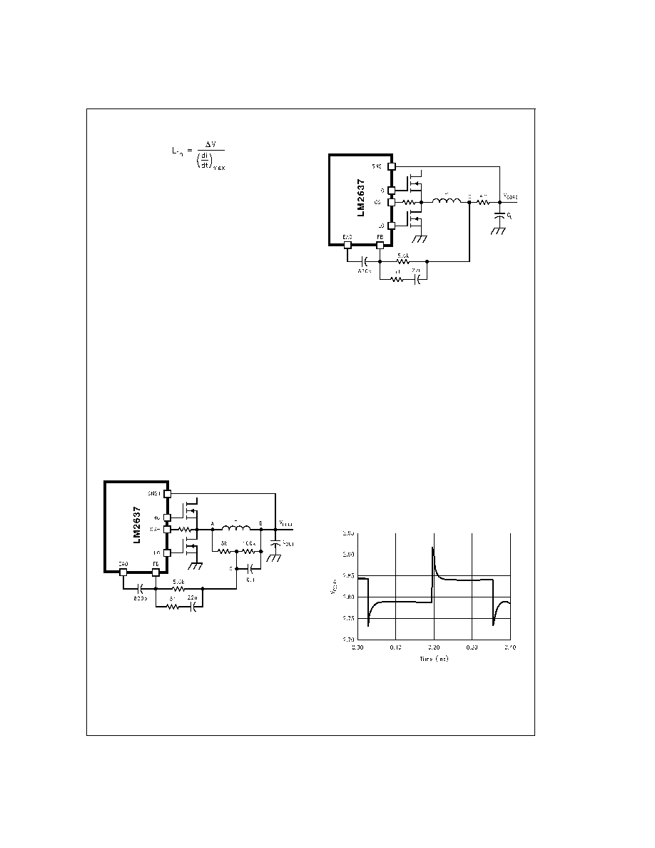
Dynamic Positioning of Load Voltage
The following is just a quick overview of a technique called
dynamic voltage positioning. For a detailed explanation and
examples please refer to our application note
Using Dy-
namic Voltage Positioning Technique to Reduce the Cost of
Output Capacitors in Advanced Microprocessor Power Sup-
plies. An associated spreadsheet is also available for auto-
mated design.
Since the typical MPU core voltage’s steady state regulation
window is fairly large, it is a good idea to dynamically posi-
tion the steady state output voltage in the steady state regu-
lation window with respect to load current level so that the
output voltage has more headroom for load transient re-
sponse. This needs load current information. There are at
least two simple ways to implement this idea with LM2637.
One is to utilize the output inductor DC resistance, see
Fig-
ure 9. The average voltage across the output inductor is ac-
tually that across its DC resistance, which is proportional to
load current.
Since the switching node voltage V
A toggles between the in-
put voltage and ground at the switching frequency, it is im-
possible to choose node A as the feedback point, otherwise
the dynamic performance will suffer and the system may
have noise problems. Using a low pass filter network around
the inductor, such as the one shown in the figure, seems to
be a good idea. The feedback point is node C.
Since at switching frequency the impedance of the 0.1 F is
much less than 5 k
, so the toggling voltage at node A will
mainly drop across the 5 k
resistor and node C will be
much quieter than A. However, V
CB average is still the ma-
jority of V
AB average, because of the ratio of the resistor di-
vider. So in steady state V
C = IO xrL +VCORE, where rL is the
inductor DC resistance. So at no load, output voltage is
equal to V
C, and at full load, output voltage is IO xrL lower
than V
C. To further utilize the steady state regulation window,
a resistor can be connected between the FB pin and ground
to increase the no-load output voltage to close to the upper
limit of the window.
A possible drawback of the scheme in
Figure 9 is slow tran-
sient recovery speed. Since the 5 k
resistor and the 0.1 F
capacitor have a large time constant, the settling of node C
to its steady state value during a load transient may take a
few milliseconds. Depends on the interaction between the
compensation network and the 0.1 F capacitor, V
CORE may
take different routes to reach its steady state value. This is
undesired when the load transient happens more than 1000
times per second. Reducing the time constant will result in a
more fluctuating V
C, due to a less effective low pass filter.
Fine tuning the parameters may generate an acceptable de-
sign.
Another way to implement the dynamic voltage ppsitioning is
through the use of a separate resistor, such as the 4 m
re-
sistor in
Figure 10 above. The advantage of this implementa-
tion over the previous one is a much faster recovery speed of
V
CORE from transient level to steady state level. A fine-tuned
compensation network will give good response as shown in
Figure 11. The disadvantage is additional power loss. The to-
tal power loss can be 0.78W at 14A of load current. The cost
of the resistor can be minimized by using a PCB etch
resistor.
PCB Layout Considerations
There are several points to consider.
DS100848-27
FIGURE 9. Dynamic Voltage Positioning by Utilizing
Output Inductor DC Resistance
DS100848-28
FIGURE 10. Dynamic Voltage Positioning by Using a
Stand-Alone Resistor
DS100848-29
FIGURE 11. Load Transient Response with DVP: 0A to
14A, ESR = 9.4 m
, Droop Resistor = 4m
www.national.com
15
相关PDF资料 |
PDF描述 |
|---|---|
| LM2639MX/NOPB | SWITCHING CONTROLLER, 8700 kHz SWITCHING FREQ-MAX, PDSO24 |
| LM2639M/NOPB | SWITCHING CONTROLLER, 8700 kHz SWITCHING FREQ-MAX, PDSO24 |
| LM2639MWC | SWITCHING CONTROLLER, 8700 kHz SWITCHING FREQ-MAX, UUC |
| LM2641-ADJMDC | DUAL SWITCHING CONTROLLER, 345 kHz SWITCHING FREQ-MAX, UUC |
| LM2645MTD/NOPB | SWITCHING CONTROLLER, 335 kHz SWITCHING FREQ-MAX, PDSO48 |
相关代理商/技术参数 |
参数描述 |
|---|---|
| LM2637MX/NOPB | 功能描述:IC MOTHERBRD PWR SUPPLY 24-SOIC RoHS:是 类别:集成电路 (IC) >> PMIC - 电源管理 - 专用 系列:- 应用说明:Ultrasound Imaging Systems Application Note 产品培训模块:Lead (SnPb) Finish for COTS Obsolescence Mitigation Program 标准包装:37 系列:- 应用:医疗用超声波成像,声纳 电流 - 电源:- 电源电压:2.37 V ~ 6 V 工作温度:0°C ~ 70°C 安装类型:表面贴装 封装/外壳:56-WFQFN 裸露焊盘 供应商设备封装:56-TQFN-EP(8x8) 包装:管件 |
| LM2638 | 制造商:未知厂家 制造商全称:未知厂家 功能描述: |
| LM2638M | 制造商:Texas Instruments 功能描述: |
| LM2638M/NOPB | 功能描述:IC MOTHERBRD PWR SUPPLY 24-SOIC RoHS:是 类别:集成电路 (IC) >> PMIC - 电源管理 - 专用 系列:- 应用说明:Ultrasound Imaging Systems Application Note 产品培训模块:Lead (SnPb) Finish for COTS Obsolescence Mitigation Program 标准包装:37 系列:- 应用:医疗用超声波成像,声纳 电流 - 电源:- 电源电压:2.37 V ~ 6 V 工作温度:0°C ~ 70°C 安装类型:表面贴装 封装/外壳:56-WFQFN 裸露焊盘 供应商设备封装:56-TQFN-EP(8x8) 包装:管件 |
| LM2638MX | 功能描述:IC MOTHERBRD PWR SUPPLY 24-SOIC RoHS:是 类别:集成电路 (IC) >> PMIC - 电源管理 - 专用 系列:- 应用说明:Ultrasound Imaging Systems Application Note 产品培训模块:Lead (SnPb) Finish for COTS Obsolescence Mitigation Program 标准包装:37 系列:- 应用:医疗用超声波成像,声纳 电流 - 电源:- 电源电压:2.37 V ~ 6 V 工作温度:0°C ~ 70°C 安装类型:表面贴装 封装/外壳:56-WFQFN 裸露焊盘 供应商设备封装:56-TQFN-EP(8x8) 包装:管件 |
发布紧急采购,3分钟左右您将得到回复。