- 您现在的位置:买卖IC网 > PDF目录98000 > LM2660MMX/NOPB (NATIONAL SEMICONDUCTOR CORP) SWITCHED CAPACITOR CONVERTER, 40 kHz SWITCHING FREQ-MAX, PDSO8 PDF资料下载
参数资料
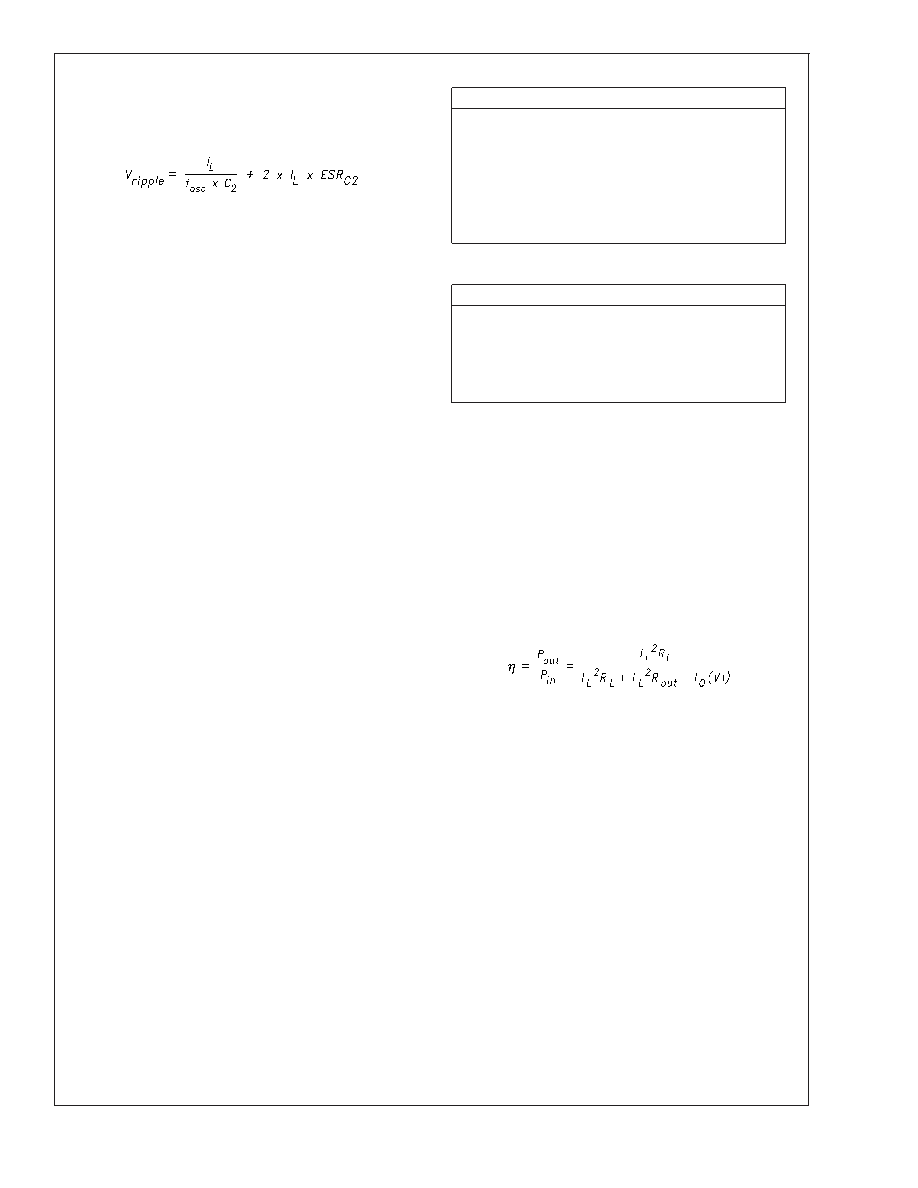
| 型号: | LM2660MMX/NOPB |
| 厂商: | NATIONAL SEMICONDUCTOR CORP |
| 元件分类: | 稳压器 |
| 英文描述: | SWITCHED CAPACITOR CONVERTER, 40 kHz SWITCHING FREQ-MAX, PDSO8 |
| 封装: | MINI, SO-8 |
| 文件页数: | 11/13页 |
| 文件大小: | 358K |
| 代理商: | LM2660MMX/NOPB |
Application Information (Continued)
The peak-to-peak output voltage ripple is determined by the
oscillator frequency, and the capacitance and ESR of the
output capacitor C
2:
Again, using a low ESR capacitor will result in lower ripple.
POSITIVE VOLTAGE DOUBLER
The LM2660/LM2661 can operate as a positive voltage dou-
bler (as shown in the Basic Application Circuits). The dou-
bling function is achieved by reversing some of the connec-
tions to the device. The input voltage is applied to the GND
pin with an allowable voltage from 2.5V to 5.5V. The V+ pin
is used as the output. The LV pin and OUT pin must be
connected to ground. The OSC pin can not be driven by an
external clock in this operation mode. The unloaded output
voltage is twice of the input voltage and is not reduced by the
diode D
1’s forward drop.
The Schottky diode D
1 is only needed for start-up. The
internal oscillator circuit uses the V+ pin and the LV pin
(connected to ground in the voltage doubler circuit) as its
power rails. Voltage across V+ and LV must be larger than
1.5V to insure the operation of the oscillator. During start-up,
D
1 is used to charge up the voltage at V+ pin to start the
oscillator; also, it protects the device from turning-on its own
parasitic diode and potentially latching-up. Therefore, the
Schottky diode D
1 should have enough current carrying
capability to charge the output capacitor at start-up, as well
as a low forward voltage to prevent the internal parasitic
diode from turning-on. A Schottky diode like 1N5817 can be
used for most applications. If the input voltage ramp is less
than 10V/ms, a smaller Schottky diode like MBR0520LT1
can be used to reduce the circuit size.
SPLIT V+ IN HALF
Another interesting application shown in the Basic Applica-
tion Circuits is using the LM2660/LM2661 as a precision
voltage divider. Since the off-voltage across each switch
equals V
IN/2, the input voltage can be raised to +11V.
CHANGING OSCILLATOR FREQUENCY
For the LM2660, the internal oscillator frequency can be
selected using the Frequency Control (FC) pin. When FC is
open, the oscillator frequency is 10 kHz; when FC is con-
nected to V+, the frequency increases to 80 kHz. A higher
oscillator frequency allows smaller capacitors to be used for
equivalent output resistance and ripple, but increases the
typical supply current from 0.12 mA to 1 mA.
The oscillator frequency can be lowered by adding an exter-
nal capacitor between OSC and GND. (See Typical Perfor-
mance Characteristics.) Also, in the inverter mode, an exter-
nal clock that swings within 100 mV of V+ and GND can be
used to drive OSC. Any CMOS logic gate is suitable for
driving OSC. LV must be grounded when driving OSC. The
maximum external clock frequency is limited to 150 kHz.
The switching frequency of the converter (also called the
charge pump frequency) is half of the oscillator frequency.
Note: OSC cannot be driven by an external clock in the voltage-doubling
mode.
TABLE 1. LM2660 Oscillator Frequency Selection
FC
OSC
Oscillator
Open
10 kHz
V+
Open
80 kHz
Open or V+
External Capacitor
See Typical
Performance
Characteristics
N/A
External Clock
(inverter mode only)
Frequency
TABLE 2. LM2661 Oscillator Frequency Selection
OSC
Oscillator
Open
80 kHz
External Capacitor
See Typical Performance
Characteristics
External Clock
External Clock Frequency
(inverter mode only)
SHUTDOWN MODE
For the LM2661, a shutdown (SD) pin is available to disable
the device and reduce the quiescent current to 0.5 A.
Applying a voltage greater than 2V to the SD pin will bring
the device into shutdown mode. While in normal operating
mode, the SD pin is connected to ground.
CAPACITOR SELECTION
As discussed in the Simple Negative Voltage Converter
section, the output resistance and ripple voltage are depen-
dent on the capacitance and ESR values of the external
capacitors. The output voltage drop is the load current times
the output resistance, and the power efficiency is
Where I
Q(V+) is the quiescent power loss of the IC device,
and I
L
2R
OUT is the conversion loss associated with the
switch on-resistance, the two external capacitors and their
ESRs.
Since the switching current charging and discharging C
1 is
approximately twice as the output current, the effect of the
ESR of the pumping capacitor C
1 is multiplied by four in the
output resistance. The output capacitor C
2 is charging and
discharging at a current approximately equal to the output
current, therefore, its ESR only counts once in the output
resistance. However, the ESR of C
2 directly affects the
output voltage ripple. Therefore, low ESR capacitors (Table
3) are recommended for both capacitors to maximize effi-
ciency, reduce the output voltage drop and voltage ripple.
For convenience, C
1 and C2 are usually chosen to be the
same.
The output resistance varies with the oscillator frequency
and the capacitors. In Figure 3, the output resistance vs.
oscillator frequency curves are drawn for three different tan-
talum capacitors. At very low frequency range, capacitance
plays the most important role in determining the output re-
sistance. Once the frequency is increased to some point
(such as 20 kHz for the 150 F capacitors), the output
resistance is dominated by the ON resistance of the internal
switches and the ESRs of the external capacitors. A low
LM2660/LM2661
www.national.com
7
相关PDF资料 |
PDF描述 |
|---|---|
| LM2661MM/NOPB | SWITCHED CAPACITOR CONVERTER, 80 kHz SWITCHING FREQ-MAX, PDSO8 |
| LM2661MMX/NOPB | SWITCHED CAPACITOR CONVERTER, 80 kHz SWITCHING FREQ-MAX, PDSO8 |
| LM2661MX/NOPB | SWITCHED CAPACITOR CONVERTER, 80 kHz SWITCHING FREQ-MAX, PDSO8 |
| LM2664MDC | SWITCHED CAPACITOR CONVERTER, 80 kHz SWITCHING FREQ-MAX, UUC |
| LM2704MFX-ADJ/NOPB | 0.62 A SWITCHING REGULATOR, PDSO5 |
相关代理商/技术参数 |
参数描述 |
|---|---|
| LM2660MX | 功能描述:电荷泵 RoHS:否 制造商:Maxim Integrated 功能:Inverting, Step Up 输出电压:- 1.5 V to - 5.5 V, 3 V to 11 V 输出电流:100 mA 电源电流:1 mA 最大工作温度:+ 70 C 封装 / 箱体:SOIC-8 Narrow 封装:Tube |
| LM2660MX/NOPB | 功能描述:电荷泵 RoHS:否 制造商:Maxim Integrated 功能:Inverting, Step Up 输出电压:- 1.5 V to - 5.5 V, 3 V to 11 V 输出电流:100 mA 电源电流:1 mA 最大工作温度:+ 70 C 封装 / 箱体:SOIC-8 Narrow 封装:Tube |
| LM2661 | 制造商:NSC 制造商全称:National Semiconductor 功能描述:Switched Capacitor Voltage Converter |
| LM2661/3/4EVAL | 功能描述:电源管理IC开发工具 LM2661/3/4 EVAL BOARD RoHS:否 制造商:Maxim Integrated 产品:Evaluation Kits 类型:Battery Management 工具用于评估:MAX17710GB 输入电压: 输出电压:1.8 V |
| LM2661/3/4EVAL/NOPB | 功能描述:电源管理IC开发工具 LM2661/3/4 EVAL BRD RoHS:否 制造商:Maxim Integrated 产品:Evaluation Kits 类型:Battery Management 工具用于评估:MAX17710GB 输入电压: 输出电压:1.8 V |
发布紧急采购,3分钟左右您将得到回复。