- 您现在的位置:买卖IC网 > PDF目录98000 > LM2661MM/NOPB (NATIONAL SEMICONDUCTOR CORP) SWITCHED CAPACITOR CONVERTER, 80 kHz SWITCHING FREQ-MAX, PDSO8 PDF资料下载
参数资料
| 型号: | LM2661MM/NOPB |
| 厂商: | NATIONAL SEMICONDUCTOR CORP |
| 元件分类: | 稳压器 |
| 英文描述: | SWITCHED CAPACITOR CONVERTER, 80 kHz SWITCHING FREQ-MAX, PDSO8 |
| 封装: | MINI, SO-8 |
| 文件页数: | 10/13页 |
| 文件大小: | 358K |
| 代理商: | LM2661MM/NOPB |
Pin Description
Pin
Name
Function
Voltage Inverter
Voltage Doubler
1
FC
Frequency control for internal oscillator:
Same as inverter.
(LM2660)
FC = open, f
OSC = 10 kHz (typ);
FC = V+, f
OSC = 80 kHz (typ);
FC has no effect when OSC pin is driven externally.
1SD
(LM2661)
Shutdown control pin, tie this pin to the ground in
normal operation, and to V+ for shutdown.
Same as inverter.
2
CAP+
Connect this pin to the positive terminal of
charge-pump capacitor.
Same as inverter.
3
GND
Power supply ground input.
Power supply positive voltage input.
4
CAP
Connect this pin to the negative terminal of
charge-pump capacitor.
Same as inverter.
5
OUT
Negative voltage output.
Power supply ground input.
6
LV
Low-voltage operation input. Tie LV to GND when
input voltage is less than 3.5V. Above 3.5V, LV can
be connected to GND or left open. When driving OSC
with an external clock, LV must be connected to
GND.
LV must be tied to OUT.
7
OSC
Oscillator control input. OSC is connected to an
internal 15 pF capacitor. An external capacitor can be
connected to slow the oscillator. Also, an external
clock can be used to drive OSC.
Same as inverter except that OSC cannot be driven
by an external clock.
8
V+
Power supply positive voltage input.
Positive voltage output.
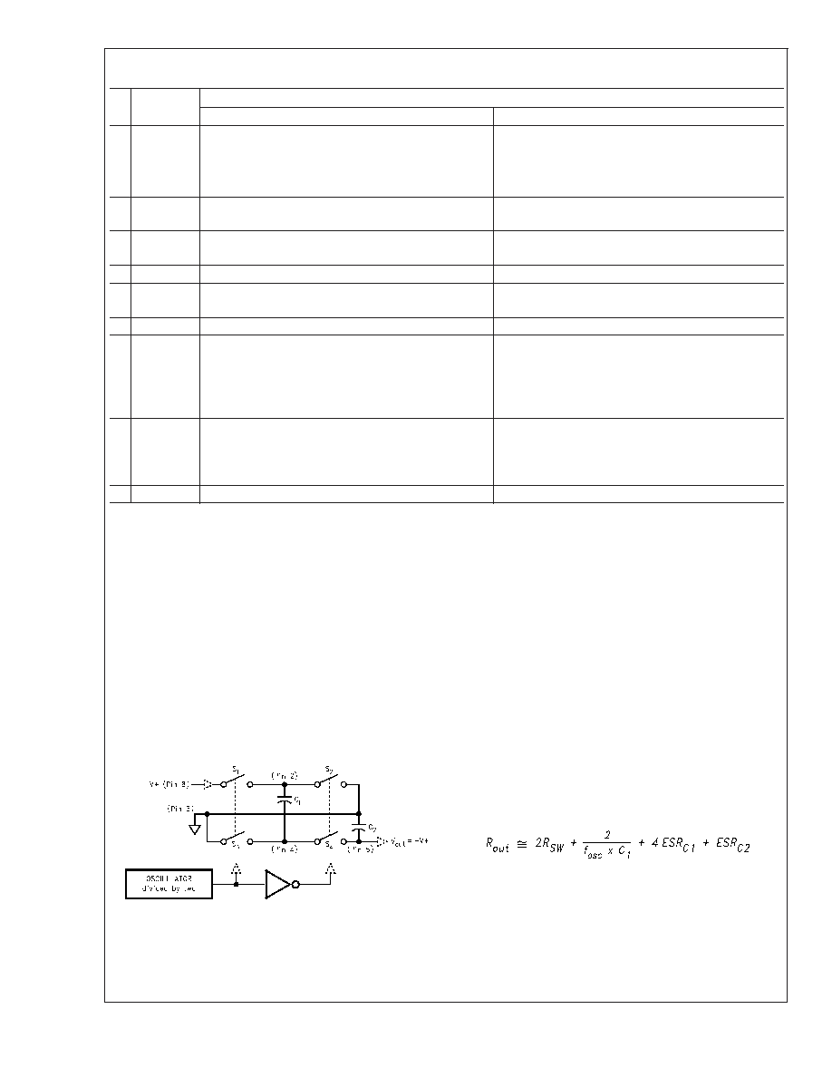
Circuit Description
The LM2660/LM2661 contains four large CMOS switches
which are switched in a sequence to invert the input supply
voltage. Energy transfer and storage are provided by exter-
nal capacitors. Figure 2 illustrates the voltage conversion
scheme. When S
1 and S3 are closed, C1 charges to the
supply voltage V+. During this time interval switches S
2 and
S
4 are open. In the second time interval, S1 and S3 are open
and S
2 and S4 are closed, C1 is charging C2. After a number
of cycles, the voltage across C
2 will be pumped to V+. Since
the anode of C
2 is connected to ground, the output at the
cathode of C
2 equals (V+) assuming no load on C2, no loss
in the switches, and no ESR in the capacitors. In reality, the
charge transfer efficiency depends on the switching fre-
quency, the on-resistance of the switches, and the ESR of
the capacitors.
Application Information
SIMPLE NEGATIVE VOLTAGE CONVERTER
The main application of LM2660/LM2661 is to generate a
negative supply voltage. The voltage inverter circuit uses
only two external capacitors as shown in the Basic Applica-
tion Circuits. The range of the input supply voltage is 1.5V to
5.5V. For a supply voltage less than 3.5V, the LV pin must be
connected to ground to bypass the internal regulator cir-
cuitry. This gives the best performance in low voltage appli-
cations. If the supply voltage is greater than 3.5V, LV may be
connected to ground or left open. The choice of leaving LV
open simplifies the direct substitution of the LM2660/
LM2661 for the LMC7660 Switched Capacitor Voltage Con-
verter.
The output characteristics of this circuit can be approximated
by an ideal voltage source in series with a resistor. The
voltage source equals (V+). The output resistance R
out is a
function of the ON resistance of the internal MOS switches,
the oscillator frequency, and the capacitance and ESR of C
1
and C
2. A good approximation is:
where R
SW is the sum of the ON resistance of the internal
MOS switches shown in Figure 2.
High value, low ESR capacitors will reduce the output resis-
tance. Instead of increasing the capacitance, the oscillator
frequency can be increased to reduce the 2/(f
osc xC1) term.
Once this term is trivial compared with R
SW and ESRs,
further increasing in oscillator frequency and capacitance will
become ineffective.
01291121
FIGURE 2. Voltage Inverting Principle
LM2660/LM2661
www.national.com
6
相关PDF资料 |
PDF描述 |
|---|---|
| LM2661MMX/NOPB | SWITCHED CAPACITOR CONVERTER, 80 kHz SWITCHING FREQ-MAX, PDSO8 |
| LM2661MX/NOPB | SWITCHED CAPACITOR CONVERTER, 80 kHz SWITCHING FREQ-MAX, PDSO8 |
| LM2664MDC | SWITCHED CAPACITOR CONVERTER, 80 kHz SWITCHING FREQ-MAX, UUC |
| LM2704MFX-ADJ/NOPB | 0.62 A SWITCHING REGULATOR, PDSO5 |
| LM2710MTX-ADJ/NOPB | 1.4 A SWITCHING REGULATOR, 1500 kHz SWITCHING FREQ-MAX, PDSO20 |
相关代理商/技术参数 |
参数描述 |
|---|---|
| LM2661MMX | 制造商:未知厂家 制造商全称:未知厂家 功能描述:DC-to-DC Voltage Converter |
| LM2661MMX/NOPB | 功能描述:IC REG MULTI CONFIG 0.1A 8MSOP RoHS:是 类别:集成电路 (IC) >> PMIC - 稳压器 - DC DC 开关稳压器 系列:- 产品培训模块:Lead (SnPb) Finish for COTS Obsolescence Mitigation Program 标准包装:1 系列:- 类型:降压(降压) 输出类型:固定 输出数:1 输出电压:3.3V 输入电压:4.5 V ~ 24 V PWM 型:- 频率 - 开关:- 电流 - 输出:125mA 同步整流器:无 工作温度:-40°C ~ 85°C 安装类型:表面贴装 封装/外壳:SOT-23-6 包装:Digi-Reel® 供应商设备封装:SOT-6 其它名称:MAX1836EUT33#TG16DKR |
| LM2661MX | 制造商:Rochester Electronics LLC 功能描述: 制造商:Texas Instruments 功能描述: |
| LM2661MX/NOPB | 功能描述:IC REG MULTI CONFIG 0.1A 8SOIC RoHS:是 类别:集成电路 (IC) >> PMIC - 稳压器 - DC DC 开关稳压器 系列:- 产品培训模块:Lead (SnPb) Finish for COTS Obsolescence Mitigation Program 标准包装:1 系列:- 类型:降压(降压) 输出类型:固定 输出数:1 输出电压:3.3V 输入电压:4.5 V ~ 24 V PWM 型:- 频率 - 开关:- 电流 - 输出:125mA 同步整流器:无 工作温度:-40°C ~ 85°C 安装类型:表面贴装 封装/外壳:SOT-23-6 包装:Digi-Reel® 供应商设备封装:SOT-6 其它名称:MAX1836EUT33#TG16DKR |
| LM2661MX_NOPB | 制造商:TI 制造商全称:Texas Instruments 功能描述:LM2660 Switched Capacitor Voltage Converter |
发布紧急采购,3分钟左右您将得到回复。