- 您现在的位置:买卖IC网 > PDF目录44551 > LM2702MT-ADJ/NOPB (NATIONAL SEMICONDUCTOR CORP) 2.6 A SWITCHING REGULATOR, 720 kHz SWITCHING FREQ-MAX, PDSO16 PDF资料下载
参数资料
| 型号: | LM2702MT-ADJ/NOPB |
| 厂商: | NATIONAL SEMICONDUCTOR CORP |
| 元件分类: | 稳压器 |
| 英文描述: | 2.6 A SWITCHING REGULATOR, 720 kHz SWITCHING FREQ-MAX, PDSO16 |
| 封装: | TSSOP-16 |
| 文件页数: | 15/21页 |
| 文件大小: | 1197K |
| 代理商: | LM2702MT-ADJ/NOPB |
Pin Functions
Vcom+(Pin 1): Positive input terminal of Vcom amplifier.
Vcom(Pin 2): Negative input terminal of Vcom amplifier.
Vcom(Pin 3): Output terminal of Vcom amplifier.
Delay(Pin 4): PMOS switch delay control pin. See Operation
section for setting the delay time.
The delay time begins when the output voltage of the DC/DC
switching regulator reaches 85% of its true output voltage.
This corresponds to a FB voltage of about 1.1V. The PMOS
switch is controlled with both the delay time and the switch
control pin, SWC. If no Cdelay capacitor is used, the PMOS
switch is controlled solely with the SWC pin.
Css(Pin 5): Softstart pin. Connect capacitor to Css pin and
AGND plane to slowly ramp inductor current on startup. See
Operation section for setting the softstart time.
V
C(Pin 6): Compensation Network for Boost switching regu-
lator. Connect resistor/capacitor network between V
C pin
and AGND for boost switching regulator AC compensation.
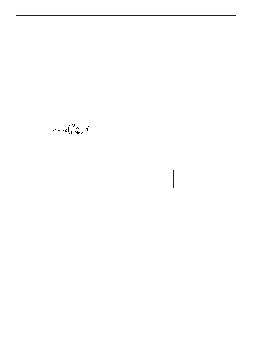
FB(Pin 7): Feedback pin. Set the output voltage by selecting
values of R1 and R2 using:
Connect the ground of the feedback network to the AGND
plane, which should be tied directly to the GND pin.
GND(Pin 8): Ground connect for LM2702. Connect all sen-
sitive circuitry, ie. feedback resistors, softstart capacitor, de-
lay capacitor, and compensation network to a dedicated
AGND plane which connects directly to this pin. Connect all
power ground components to a PGND plane which should
also connect directly to this pin. Please see Layout Consid-
erations under the Operation section for more details on
layout suggestions.
SW(Pin 9): This is the drain of the internal NMOS power
switch. Minimize the metal trace area connected to this pin to
minimize EMI.
V
IN(Pin 10): Input Supply Pin. Bypass this pin with a capaci-
tor as close to the device as possible. The capacitor should
connect between V
IN and GND.
SWI(Pin 11): PMOS switch input. Source connection of
PMOS device.
SWO(Pin 12): PMOS switch output. Drain connection of
PMOS device.
SWC(Pin13): PMOS switch control pin. This pin creates an
AND function with the delay time after the output of the
switching regulator has reached 85% of its nominal value. To
ensure the PMOS switch is in the correct state, apply a
voltage above 1.5V to this pin to turn on the PMOS switch
and apply a voltage below 0.7V to turn off the PMOS switch.
AV
IN(Pin 14): Supply pin for the Vcom opamp and the
Gamma buffer. Bypass this pin with a capacitor as close to
the device as possible, about 100nF. The capacitor should
connect between AV
IN and PGND.
GMA(Pin 15): Gamma Buffer output pin.
GMA+(Pin 16): Gamma Buffer input pin.
Ordering Information
Order Number
Package Type
NSC Package Drawing
Supplied As
LM2702MT-ADJ
TSSOP-16
MTC16
73 Units, Rail
LM2702MTX-ADJ
TSSOP-16
MTC16
2500 Units, Tape and Reel
LM2702
www.national.com
3
相关PDF资料 |
PDF描述 |
|---|---|
| LM27402SQX | SWITCHING CONTROLLER, 1350 kHz SWITCHING FREQ-MAX, QCC16 |
| LM27402MHX | SWITCHING CONTROLLER, 1350 kHz SWITCHING FREQ-MAX, PDSO16 |
| LM2770SD-12157/NOPB | SWITCHED CAPACITOR REGULATOR, 925 kHz SWITCHING FREQ-MAX, DSO10 |
| LM2770SDX-1215/NOPB | SWITCHED CAPACITOR REGULATOR, 925 kHz SWITCHING FREQ-MAX, DSO10 |
| LM2788MM-2.0/NOPB | SWITCHED CAPACITOR REGULATOR, 500 kHz SWITCHING FREQ-MAX, PDSO8 |
相关代理商/技术参数 |
参数描述 |
|---|---|
| LM2702MTX-ADJ | 制造商:NSC 制造商全称:National Semiconductor 功能描述:TFT Panel Module |
| LM2703 | 制造商:NSC 制造商全称:National Semiconductor 功能描述:Micropower Step-up DC/DC Converter with 350mA Peak Current Limit |
| LM2703EV | 功能描述:电源管理IC开发工具 LM2703 EVAL UNIT RoHS:否 制造商:Maxim Integrated 产品:Evaluation Kits 类型:Battery Management 工具用于评估:MAX17710GB 输入电压: 输出电压:1.8 V |
| LM2703EV/NOPB | 制造商:Texas Instruments 功能描述:Evaluation Board For LM2703 |
| LM2703MFADJ | 制造商:Texas Instruments 功能描述: |
发布紧急采购,3分钟左右您将得到回复。