参数资料
| 型号: | LM2902PWR |
| 厂商: | Rohm Semiconductor |
| 文件页数: | 7/20页 |
| 文件大小: | 0K |
| 描述: | IC OPAMP QUAD 26V 14TSSOP |
| 标准包装: | 2,500 |
| 系列: | Trophy |
| 放大器类型: | 通用 |
| 电路数: | 4 |
| 转换速率: | 0.5 V/µs |
| 增益带宽积: | 1.2MHz |
| 电流 - 输入偏压: | 20nA |
| 电压 - 输入偏移: | 3000µV |
| 电流 - 电源: | 1.4mA |
| 电流 - 输出 / 通道: | 60mA |
| 电压 - 电源,单路/双路(±): | 3 V ~ 26 V,±1.5 V ~ 13 V |
| 工作温度: | -40°C ~ 125°C |
| 安装类型: | 表面贴装 |
| 封装/外壳: | 14-TSSOP(0.173",4.40mm 宽) |
| 供应商设备封装: | 14-TSSOP |
| 包装: | 带卷 (TR) |
Technical Note
15/17
LM358DR/PWR/DGKR,LM2904DR/PWR/DGKR/VQDR/VQPWR
LM324DR/PWR/KDR,LM2902DR/PER/KDR/KPWR/KVQDR/KVQPWR
www.rohm.com
2011.06 - Rev.B
2011 ROHM Co., Ltd. All rights reserved.
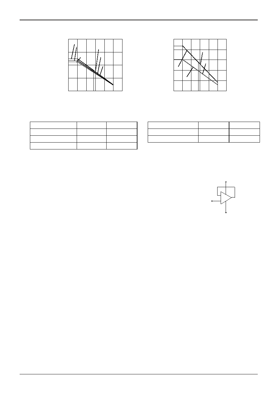
●Derating Curves
Power Dissipation
Package
Pd[W]
θja [℃/W]
Package
Pd[W]
θja [℃/W]
SOIC8 (*8)
450
3.6
SOIC14
610
4.9
TSSOP8 (*6)
500
4.0
TSSOP14
870
7.0
MSOP8/VSSOP8 (*7)
470
3.76
●Precautions
1) Unused circuits
When there are unused circuits, it is recommended that they be connected as in Figure 103,
setting the non-inverting input terminal to a potential within the in-phase input voltage range (VICR).
2) Input terminal voltage
Applying GND + 32V to the input terminal is possible without causing deterioration of the electrical
characteristics or destruction, irrespective of the supply voltage. However, this does not ensure
normal circuit operation.
Please note that the circuit operates normally only when the input voltage is within the common mode
input voltage range of the electric characteristics.
3) Power supply (single / dual)
The op-amp operates when the voltage is applied between Vcc and GND.
Therefore, the single supply op-amp can be used as a dual supply op-amp as well.
4) Power dissipation (Pd)
Using the unit in excess of the rated power dissipation may cause deterioration in electrical characteristics due to the rise of chip temperature, including
reduced current capability. Therefore, please take into consideration the power dissipation (Pd) under the actual operating conditions and apply a sufficient
margin in thermal design. Refer to the thermal derating curves for more information.
5) Short-circuits between pins and erroneous mounting
Incorrect mounting may damage the IC. In addition, the presence of foreign substances between the outputs, the output and the power supply, or the output
and GND may also result in IC destruction.
6) Operation in a strong electromagnetic field
Operation in a strong electromagnetic field may cause malfunctions.
7) Radiation
This IC is not designed to withstand radiation.
8) IC handing
Applying mechanical stress to the IC by deflecting or bending the board may cause fluctuation of the electrical characteristics due to piezoelectric (piezo)
effects.
9) IC operation
The output stage of the IC is configured using Class C push-pull circuits. Therefore, when the load resistor is connected to the middle potential of Vcc and
GND, crossover distortion occurs at the changeover between discharging and charging of the output current. Connecting a resistor between the output
terminal and GND and increasing the bias current for Class A operation will suppress crossover distortion.
10) Board inspection
Connecting a capacitor to a pin with low impedance may stress the IC. Therefore, discharging the capacitor after every process is recommended. In addition,
when attaching and detaching the jig during the inspection phase, ensure that the power is turned OFF before inspection and removal. Furthermore, please
take measures against ESD in the assembly process as well as during transportation and storage.
11) Output capacitor
Discharge of the external output capacitor to Vcc is possible via internal parasitic elements when Vcc is shorted to GND, causing damage to the internal
circuitry due to thermal stress. Therefore, when using this IC in circuits where oscillation due to output capacitive load does not occur, such as in voltage
comparators, use an output capacitor with a capacitance less than 0.1
μF.
0
200
400
600
800
1000
0
25
50
75
100
125
150
AMBIENT TEMPERATURE [℃]
P
O
W
E
R
D
IS
S
IP
A
T
IO
N
P
d
[m
W
]
0
200
400
600
800
0
25
50
75
100
125
150
AMBIENT TEMPERATURE [℃]
P
O
W
E
R
D
IS
S
IP
A
T
IO
N
P
d
[m
W
]
connect
to V icm
Vcc
GND
-
+
LM358DR/PWR/DGKR
LM2904DR/PWR/DGKR/VQDR/VQPWR
LM324DR/PWR/KDR
LM2902DR/PWR/KDR/KPWR/KQDR/KQPWR
Fig.102 Derating Curves
Fig.103 Disable circuit example
θja = (Tj-Ta)/Pd[℃/W]
70
LM358DGKR
LM358DR
LM2904PWR
LM2904VQPWR
LM2904DGKR
LM2904DR
LM2904VQDR
LM324PWR
LM324DR
LM324KDR
LM2902PWR
LM2902KPWR
LM2902KQVPWR
LM2902DR
LM2902KDR
LM2902KQVDR
70
LM358PWR
相关PDF资料 |
PDF描述 |
|---|---|
| LM2904MX | IC OPAMP DUAL 8-SOP |
| LM308H/NOPB | IC OP AMP TO-99-8 |
| LM324DT | IC OPAMP QUAD 32V 14SOIC |
| LM324MX | IC OPAMP QUAD 16/32V 14-SOP |
| LM324MX | IC OPAMP QUAD 32V 14SOIC |
相关代理商/技术参数 |
参数描述 |
|---|---|
| LM2902PWR | 制造商:Texas Instruments 功能描述:OP AMP QUAD LIN SMD ((NW)) |
| LM2902PWR | 制造商:Texas Instruments 功能描述:IC OP-AMP 1.2MHZ 0.5V/ TSSOP-14 制造商:Texas Instruments 功能描述:IC, OP-AMP, 1.2MHZ, 0.5V/s, TSSOP-14 |
| LM2902PWRE4 | 功能描述:运算放大器 - 运放 Quad General-Purpose Op Amp RoHS:否 制造商:STMicroelectronics 通道数量:4 共模抑制比(最小值):63 dB 输入补偿电压:1 mV 输入偏流(最大值):10 pA 工作电源电压:2.7 V to 5.5 V 安装风格:SMD/SMT 封装 / 箱体:QFN-16 转换速度:0.89 V/us 关闭:No 输出电流:55 mA 最大工作温度:+ 125 C 封装:Reel |
| LM2902PWRG3 | 功能描述:运算放大器 - 运放 Quadruple Op Amp RoHS:否 制造商:STMicroelectronics 通道数量:4 共模抑制比(最小值):63 dB 输入补偿电压:1 mV 输入偏流(最大值):10 pA 工作电源电压:2.7 V to 5.5 V 安装风格:SMD/SMT 封装 / 箱体:QFN-16 转换速度:0.89 V/us 关闭:No 输出电流:55 mA 最大工作温度:+ 125 C 封装:Reel |
| LM2902PWRG4 | 功能描述:运算放大器 - 运放 Quad General-Purpose Op Amp RoHS:否 制造商:STMicroelectronics 通道数量:4 共模抑制比(最小值):63 dB 输入补偿电压:1 mV 输入偏流(最大值):10 pA 工作电源电压:2.7 V to 5.5 V 安装风格:SMD/SMT 封装 / 箱体:QFN-16 转换速度:0.89 V/us 关闭:No 输出电流:55 mA 最大工作温度:+ 125 C 封装:Reel |
发布紧急采购,3分钟左右您将得到回复。