- 您现在的位置:买卖IC网 > PDF目录378651 > LM2904 (Intersil Corporation) Dual, 1MHz, Operational Amplifiers(1MHz 双路运算放大器) PDF资料下载
参数资料
| 型号: | LM2904 |
| 厂商: | Intersil Corporation |
| 元件分类: | 运动控制电子 |
| 英文描述: | Dual, 1MHz, Operational Amplifiers(1MHz 双路运算放大器) |
| 中文描述: | 双通道,1MHz的,运算放大器(1MHz的双路运算放大器) |
| 文件页数: | 2/7页 |
| 文件大小: | 85K |
| 代理商: | LM2904 |
2
Absolute Maximum Ratings
Thermal Information
Supply Voltage
CA2904, LM2904 . . . . . . . . . . . . . . . . . . . . . . . . . . . 26V or
±
13V
Other Types . . . . . . . . . . . . . . . . . . . . . . . . . . . . . . . 32V or
±
16V
Differential Input Voltage (All Types) . . . . . . . . . . . . . . . . . . . . . 32V
Input Voltage . . . . . . . . . . . . . . . . . . . . . . . . . . . . . . . . . .-0.3V to V+
Input Current (V
I
< -0.3V, Note 1) . . . . . . . . . . . . . . . . . . . . . . 50mA
Output Short Circuit Duration (V+
≤
15V, Note 2) . . . . . .Continuous
Operating Conditions
Temperature Range
CA158, CA158A. . . . . . . . . . . . . . . . . . . . . . . . . . -55
o
C to 125
o
C
CA258, . . . . . . . . . . . . . . . . . . . . . . . . . . . . . . . . . -25
o
C to 85
o
C
CA2904, LM2904 . . . . . . . . . . . . . . . . . . . . . . . . . . -40
o
C to 85
o
C
CA358, CA358A, LM358 . . . . . . . . . . . . . . . . . . . . . .0
o
C to 70
o
C
Thermal Resistance (Typical, Note 3)
PDIP Package . . . . . . . . . . . . . . . . . . .
SOIC Package . . . . . . . . . . . . . . . . . . .
Can Package . . . . . . . . . . . . . . . . . . . .
Maximum Junction Temperature (Can Package). . . . . . . . . . .175
o
C
Maximum Junction Temperature (Plastic Package). . . . . . . . .150
o
C
Maximum Storage Temperature Range. . . . . . . . . . -65
o
C to 150
o
C
Maximum Lead Temperature (Soldering 10s) . . . . . . . . . . . . 300
o
C
(SOIC - Lead Tips Only)
θ
JA
(
o
C/W)
130
170
155
θ
JC
(
o
C/W)
N/A
N/A
67
CAUTION: Stresses above those listed in “Absolute Maximum Ratings” may cause permanent damage to the device. This is a stress only rating and operation of the
device at these or any other conditions above those indicated in the operational sections of this specification is not implied.
NOTES:
1. This input current will only exist when the voltage at any of the input leads is driven negative. This current is due to the collector base junction of the
input PNP transistors becoming forward biased and thereby acting as input diode clamps. In addition to this diode action, there is also lateral NPN
parasitic transistor action on the IC chip. This transistor action can cause the output voltages of the amplifiers to go to the V+ voltage level (or to
ground for a large overdrive) for the time duration that an input is driven negative. This transistor action is not destructive and normal output states
will re-establish when the input voltage, which was negative, again returns to a value greater than -0.3V.
2. The maximum output current is approximately 40mA independent of the magnitude of V+. Continuous short circuits at V+ > 15V can cause
excessive power dissipation and eventual destruction. Short circuits from the output to V+ can cause overheating and eventual destruction of
the device. Destructive dissipation can result from simultaneous short circuits on both amplifiers.
3.
θ
JA
is measured with the component mounted on an evaluation PC board in free air.
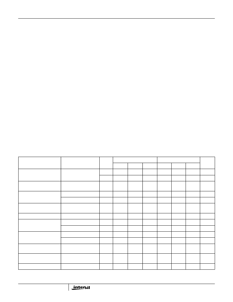
Electrical Specifications
Values Apply for Each Operational Amplifier. Supply Voltage V+ = 5V, V- = 0V,
Unless Otherwise Specified
PARAMETER
TEST CONDITIONS
TEMP
(
o
C)
CA158A
CA358A
UNITS
MIN
TYP
MAX
MIN
TYP
MAX
Input Offset
Voltage (Note 6)
25
-
1
2
-
2
3
mV
Full
-
-
4
-
-
5
mV
Average Input Offset Voltage
Drift
R
S
= 0
Full
-
7
15
-
7
20
μ
V/
o
C
Input Common Mode Voltage
Range (Note 5)
V+ = 30V
25
0
-
V+ -1.5
0
-
V+ -1.5
V
V+ = 30V
Full
0
-
V+ -2
0
-
V+ -2
V
Common Mode
Rejection Ratio
DC
25
70
85
-
65
85
-
dB
Power Supply Rejection Ratio DC
25
65
100
-
65
100
-
dB
Input Bias
Current (Note 4)
I
I
+ or I
I
-
25
-
20
50
-
45
100
nA
I
I
+ or I
I
-
Full
-
40
100
-
40
200
nA
Input Offset
Current
I
I
+ - I
I
-
25
-
2
10
-
5
30
nA
I
I
+ - I
I
-
Full
-
-
30
-
-
75
nA
Average Input Offset Current
Drift
Full
-
10
200
-
10
300
pA/
o
C
Large Signal Voltage Gain
R
L
≥
2k
, V+ = 15V (For
Large V
O
Swing)
25
50
100
-
25
100
-
kV/V
Output Voltage Swing
R
L
= 2k
25
0
-
V+ -1.5
0
-
V+ -1.5
V
CA158, CA158A, CA258, CA258A, CA358, CA358A, CA2904, LM358, LM2904
相关PDF资料 |
PDF描述 |
|---|---|
| LM2904 | Dual Operational Amplifier(双通道运算放大器) |
| LM358 | Dual Operational Amplifier(双通道运算放大器) |
| LM358A | Dual Operational Amplifier(双通道运算放大器) |
| LM2931A | Octal Transparent D-Type Latches With 3-State Outputs 20-TVSOP -40 to 85 |
| LM2931AZ5 | Octal Transparent D-Type Latches With 3-State Outputs 20-TSSOP -40 to 85 |
相关代理商/技术参数 |
参数描述 |
|---|---|
| LM2904_07 | 制造商:STMICROELECTRONICS 制造商全称:STMicroelectronics 功能描述:Low power dual operational amplifier |
| LM2904_08 | 制造商:STMICROELECTRONICS 制造商全称:STMicroelectronics 功能描述:Low power dual operational amplifier |
| LM2904A | 制造商:ONSEMI 制造商全称:ON Semiconductor 功能描述:Single Supply Dual Operational Amplifiers |
| LM2904ADMG | 功能描述:运算放大器 - 运放 3-26V Dual Lo PWR -40 to 105deg C RoHS:否 制造商:STMicroelectronics 通道数量:4 共模抑制比(最小值):63 dB 输入补偿电压:1 mV 输入偏流(最大值):10 pA 工作电源电压:2.7 V to 5.5 V 安装风格:SMD/SMT 封装 / 箱体:QFN-16 转换速度:0.89 V/us 关闭:No 输出电流:55 mA 最大工作温度:+ 125 C 封装:Reel |
| LM2904ADMR2 | 功能描述:运算放大器 - 运放 3-26V Dual Lo PWR RoHS:否 制造商:STMicroelectronics 通道数量:4 共模抑制比(最小值):63 dB 输入补偿电压:1 mV 输入偏流(最大值):10 pA 工作电源电压:2.7 V to 5.5 V 安装风格:SMD/SMT 封装 / 箱体:QFN-16 转换速度:0.89 V/us 关闭:No 输出电流:55 mA 最大工作温度:+ 125 C 封装:Reel |
发布紧急采购,3分钟左右您将得到回复。