- 您现在的位置:买卖IC网 > PDF目录39247 > LM2907N-8EP (NATIONAL SEMICONDUCTOR CORP) VOLTAGE-FREQUENCY CONVERTER, PDIP8 PDF资料下载
参数资料
| 型号: | LM2907N-8EP |
| 厂商: | NATIONAL SEMICONDUCTOR CORP |
| 元件分类: | 模拟专用变换器 |
| 英文描述: | VOLTAGE-FREQUENCY CONVERTER, PDIP8 |
| 封装: | PLASTIC, DIP-8 |
| 文件页数: | 19/21页 |
| 文件大小: | 715K |
| 代理商: | LM2907N-8EP |
Applications Information
The LM2907EP series of tachometer circuits is designed for
minimum external part count applications and maximum ver-
satility. In order to fully exploit its features and advantages
let’s examine its theory of operation. The first stage of op-
eration is a differential amplifier driving a positive feedback
flip-flop circuit. The input threshold voltage is the amount of
differential input voltage at which the output of this stage
changes state. Two options (LM2907-8EP, LM2917-8EP)
have one input internally grounded so that an input signal
must swing above and below ground and exceed the input
thresholds to produce an output. This is offered specifically
for magnetic variable reluctance pickups which typically pro-
vide a single-ended ac output. This single input is also fully
protected against voltage swings to ±28V, which are easily
attained with these types of pickups.
The differential input options (LM2907EP, LM2917EP) give
the user the option of setting his own input switching level
and still have the hysteresis around that level for excellent
noise rejection in any application. Of course in order to allow
the inputs to attain common-mode voltages above ground,
input protection is removed and neither input should be
taken outside the limits of the supply voltage being used. It is
very important that an input not go below ground without
some resistance in its lead to limit the current that will then
flow in the epi-substrate diode.
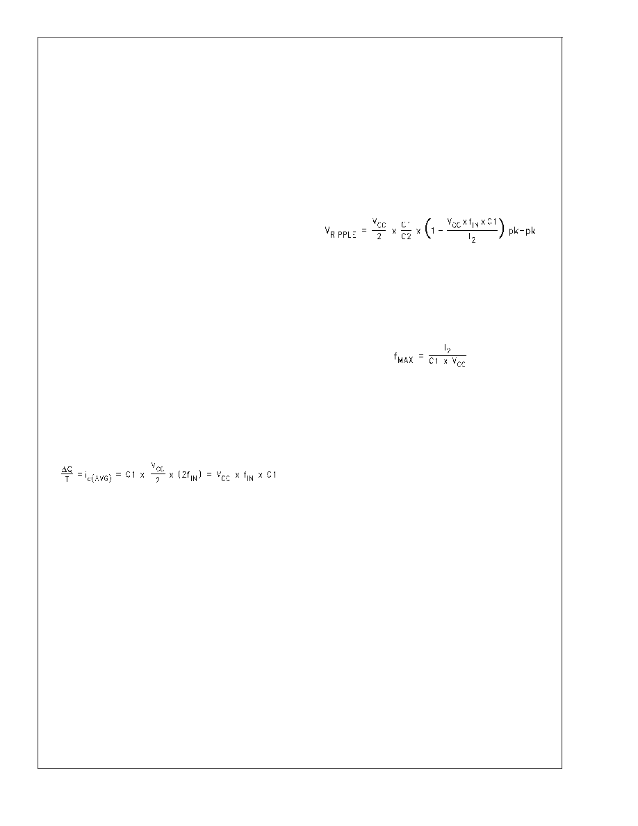
Following the input stage is the charge pump where the input
frequency is converted to a dc voltage. To do this requires
one timing capacitor, one output resistor, and an integrating
or filter capacitor. When the input stage changes state (due
to a suitable zero crossing or differential voltage on the input)
the timing capacitor is either charged or discharged linearly
between two voltages whose difference is V
CC/2. Then in
one half cycle of the input frequency or a time equal to 1/2 f
IN
the change in charge on the timing capacitor is equal to
V
CC/2 x C1. The average amount of current pumped into or
out of the capacitor then is:
The output circuit mirrors this current very accurately into the
load resistor R1, connected to ground, such that if the pulses
of current are integrated with a filter capacitor, then V
O =ic x
R1, and the total conversion equation becomes:
V
O =VCC xfIN xC1xR1xK
Where K is the gain constant — typically 1.0.
The size of C2 is dependent only on the amount of ripple
voltage allowable and the required response time.
CHOOSING R1 AND C1
There are some limitations on the choice of R1 and C1 which
should be considered for optimum performance. The timing
capacitor also provides internal compensation for the charge
pump and should be kept larger than 500 pF for very accu-
rate operation. Smaller values can cause an error current on
R1, especially at low temperatures. Several considerations
must be met when choosing R1. The output current at pin 3
is internally fixed and therefore V
O/R1 must be less than or
equal to this value. If R1 is too large, it can become a
significant fraction of the output impedance at pin 3 which
degrades linearity. Also output ripple voltage must be con-
sidered and the size of C2 is affected by R1. An expression
that describes the ripple content on pin 3 for a single R1C2
combination is:
It appears R1 can be chosen independent of ripple, however
response time, or the time it takes V
OUT to stabilize at a new
voltage increases as the size of C2 increases, so a compro-
mise between ripple, response time, and linearity must be
chosen carefully.
As a final consideration, the maximum attainable input fre-
quency is determined by V
CC, C1 and I2:
USING ZENER REGULATED OPTIONS (LM2917EP)
For those applications where an output voltage or current
must be obtained independent of supply voltage variations,
the LM2917EP is offered. The most important consideration
in choosing a dropping resistor from the unregulated supply
to the device is that the tachometer and op amp circuitry
alone require about 3 mA at the voltage level provided by the
zener. At low supply voltages there must be some current
flowing in the resistor above the 3 mA circuit current to
operate the regulator. As an example, if the raw supply
varies from 9V to 16V, a resistance of 470
will minimize the
zener voltage variation to 160 mV. If the resistance goes
under 400
or over 600 the zener variation quickly rises
above 200 mV for the same input variation.
LM2907EP/LM2917EP
Enhanced
Plastic
www.national.com
7
相关PDF资料 |
PDF描述 |
|---|---|
| LM2917N-8EP | VOLTAGE-FREQUENCY CONVERTER, PDIP8 |
| LM2917MEP | VOLTAGE-FREQUENCY CONVERTER, PDSO14 |
| LM2907MXEP | VOLTAGE-FREQUENCY CONVERTER, PDSO14 |
| LM2907M-8EP | VOLTAGE-FREQUENCY CONVERTER, PDSO8 |
| LM2917NEP | VOLTAGE-FREQUENCY CONVERTER, PDIP14 |
相关代理商/技术参数 |
参数描述 |
|---|---|
| LM290N | 制造商:STMicroelectronics 功能描述:290N |
| LM290WW1-SSA1 | 制造商:LG.Philips Lcd 功能描述:29" 21:9 (2560 X 1080), 300 NITS, LVDS, SRGB - Bulk |
| LM2917AN | 制造商:Texas Instruments 功能描述: |
| LM2917M | 功能描述:电压频率转换及频率电压转换 RoHS:否 制造商:Texas Instruments 全标度频率:4000 KHz 线性误差:+/- 1 % FSR 电源电压-最大: 电源电压-最小: 最大工作温度:+ 85 C 最小工作温度:- 25 C 安装风格:Through Hole 封装 / 箱体:PDIP-14 封装:Tube |
| LM2917M/NOPB | 功能描述:电压频率转换及频率电压转换 FREQ TO VLTG CONVERTER RoHS:否 制造商:Texas Instruments 全标度频率:4000 KHz 线性误差:+/- 1 % FSR 电源电压-最大: 电源电压-最小: 最大工作温度:+ 85 C 最小工作温度:- 25 C 安装风格:Through Hole 封装 / 箱体:PDIP-14 封装:Tube |
发布紧急采购,3分钟左右您将得到回复。