- 您现在的位置:买卖IC网 > PDF目录39247 > LM2917MX-8EP (NATIONAL SEMICONDUCTOR CORP) VOLTAGE-FREQUENCY CONVERTER, PDSO8 PDF资料下载
参数资料
| 型号: | LM2917MX-8EP |
| 厂商: | NATIONAL SEMICONDUCTOR CORP |
| 元件分类: | 模拟专用变换器 |
| 英文描述: | VOLTAGE-FREQUENCY CONVERTER, PDSO8 |
| 封装: | 0.150 INCH, PLASTIC, SOP-8 |
| 文件页数: | 15/21页 |
| 文件大小: | 715K |
| 代理商: | LM2917MX-8EP |
Absolute Maximum Ratings (Note 4)
If Military/Aerospace specified devices are required,
please contact the National Semiconductor Sales Office/
Distributors for availability and specifications.
Supply Voltage
28V
Collector Voltage
28V
Differential Input Voltage
Tachometer
28V
Op Amp/Comparator
28V
Input Voltage Range
Tachometer
LM2907-8EP, LM2917-8EP
±28V
LM2907EP, LM2917EP
0.0V to +28V
Op Amp/Comparator
0.0V to +28V
Power Dissipation (Note 4)
LM2907-8EP, LM2917-8EP
1200 mW
LM2907-14EP, LM2917-14EP
1580 mW
Operating Temperature Range
40C to +85C
Storage Temperature Range
65C to +150C
Soldering Information
Dual-In-Line Package
Soldering (10 seconds)
260C
Small Outline Package
Vapor Phase (60 seconds)
215C
Infrared (15 seconds)
220C
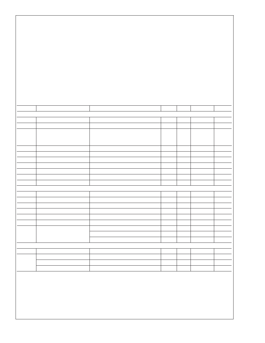
Electrical Characteristics V
CC =12VDC,TA = 25C, see test circuit
Symbol
Parameter
Conditions
Min
Typ
Max
Units
TACHOMETER
Input Thresholds
V
±10
±25
±40
mV
Hysteresis
V
30
mV
Offset Voltage
V
LM2907EP/LM2917EP
3.5
10
mV
LM2907-8EP/LM2917-8EP
5
15
mV
Input Bias Current
V
IN = ±50 mVDC
0.1
1
A
V
OH
Pin 2
V
8.3
V
OL
Pin 2
V
2.3
V
I
2,I3
Output Current
V2 = V3 = 6.0V (Note 7)
140
180
240
A
I
3
Leakage Current
I2 = 0, V3 = 0
0.1
A
K
Gain Constant
0.9
1.0
1.1
Linearity
f
IN = 1 kHz, 5 kHz, 10 kHz (Note 8)
1.0
0.3
+1.0
%
OP/AMP COMPARATOR
V
OS
V
IN = 6.0V
3
10
mV
I
BIAS
V
IN = 6.0V
50
500
nA
Input Common-Mode Voltage
0
V
CC1.5V
V
Voltage Gain
200
V/mV
Output Sink Current
V
C = 1.0
40
50
mA
Output Source Current
V
E =VCC 2.0
10
mA
Saturation Voltage
I
SINK = 5 mA
0.1
0.5
V
I
SINK =20mA
1.0
V
I
SINK = 50 mA
1.0
1.5
V
ZENER REGULATOR
Regulator Voltage
R
DROP = 470
7.56
V
Series Resistance
10.5
15
Temperature Stability
+1
mV/C
Total Supply Current
3.8
6
mA
Note 4: For operation in ambient temperatures above 25C, the device must be derated based on a 150C maximum junction temperature and a thermal resistance
of 101C/W junction to ambient for LM2907-8EP and LM2917-8EP, and 79C/W junction to ambient for LM2907-14EP and LM2917-14EP.
Note 5: Hysteresis is the sum +VTH (VTH), offset voltage is their difference. See test circuit.
Note 6: VOH is equal to 34 xVCC 1VBE,VOL is equal to 14 xVCC 1VBE therefore VOH VOL =VCC/2. The difference, VOH VOL, and the mirror gain, I2/I3,
are the two factors that cause the tachometer gain constant to vary from 1.0.
Note 7: Be sure when choosing the time constant R1 x C1 that R1 is such that the maximum anticipated output voltage at pin 3 can be reached with I3 x R1. The
maximum value for R1 is limited by the output resistance of pin 3 which is greater than 10 M
typically.
Note 8: Nonlinearity is defined as the deviation of VOUT (@ pin 3) for fIN = 5 kHz from a straight line defined by the VOUT @ 1 kHz and VOUT @ 10 kHz. C1 = 1000 pF,
R1 = 68k and C2 = 0.22 mFd.
LM2907EP/LM2917EP
Enhanced
Plastic
www.national.com
3
相关PDF资料 |
PDF描述 |
|---|---|
| LM2917M-8EP | VOLTAGE-FREQUENCY CONVERTER, PDSO8 |
| LM2907N-8EP | VOLTAGE-FREQUENCY CONVERTER, PDIP8 |
| LM2917N-8EP | VOLTAGE-FREQUENCY CONVERTER, PDIP8 |
| LM2917MEP | VOLTAGE-FREQUENCY CONVERTER, PDSO14 |
| LM2907MXEP | VOLTAGE-FREQUENCY CONVERTER, PDSO14 |
相关代理商/技术参数 |
参数描述 |
|---|---|
| LM2917N | 功能描述:电压频率转换及频率电压转换 RoHS:否 制造商:Texas Instruments 全标度频率:4000 KHz 线性误差:+/- 1 % FSR 电源电压-最大: 电源电压-最小: 最大工作温度:+ 85 C 最小工作温度:- 25 C 安装风格:Through Hole 封装 / 箱体:PDIP-14 封装:Tube |
| LM2917N | 制造商:Texas Instruments 功能描述:TACHO F/V CONVERTER 2917 DIP14 |
| LM2917N/NOPB | 功能描述:电压频率转换及频率电压转换 FREQ TO VLTG CONVERTER RoHS:否 制造商:Texas Instruments 全标度频率:4000 KHz 线性误差:+/- 1 % FSR 电源电压-最大: 电源电压-最小: 最大工作温度:+ 85 C 最小工作温度:- 25 C 安装风格:Through Hole 封装 / 箱体:PDIP-14 封装:Tube |
| LM2917N-8 | 功能描述:电压频率转换及频率电压转换 RoHS:否 制造商:Texas Instruments 全标度频率:4000 KHz 线性误差:+/- 1 % FSR 电源电压-最大: 电源电压-最小: 最大工作温度:+ 85 C 最小工作温度:- 25 C 安装风格:Through Hole 封装 / 箱体:PDIP-14 封装:Tube |
| LM2917N-8 | 制造商:Texas Instruments 功能描述:IC TACHO F/V CONVERTER 2917 DIP8 |
发布紧急采购,3分钟左右您将得到回复。