参数资料
| 型号: | LM317BD2TG |
| 厂商: | ON Semiconductor |
| 文件页数: | 2/12页 |
| 文件大小: | 0K |
| 描述: | IC REG LDO ADJ .5A D2PAK |
| 标准包装: | 50 |
| 稳压器拓扑结构: | 正,可调式 |
| 输出电压: | 1.2 V ~ 37 V |
| 输入电压: | 最高 40 V |
| 稳压器数量: | 1 |
| 电流 - 输出: | 500mA |
| 电流 - 限制(最小): | 1.5A |
| 工作温度: | -40°C ~ 125°C |
| 安装类型: | 表面贴装 |
| 封装/外壳: | TO-263-3,D²Pak(2 引线+接片),TO-263AB |
| 供应商设备封装: | D2PAK |
| 包装: | 管件 |
| 产品目录页面: | 1127 (CN2011-ZH PDF) |
| 其它名称: | LM317BD2TG-ND LM317BD2TGOS |
�� �
�
�LM317,� NCV317�
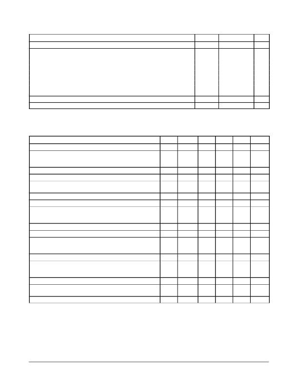
�MAXIMUM� RATINGS�
�Input� ?� Output� Voltage� Differential�
�Rating�
�Symbol�
�V� I� ?� V� O�
�Value�
�?� 0.3� to� 40�
�Unit�
�Vdc�
�Power� Dissipation�
�Case� 221A�
�T� A� =� +25� ?� C�
�Thermal� Resistance,� Junction� ?� to� ?� Ambient�
�Thermal� Resistance,� Junction� ?� to� ?� Case�
�Case� 936� (D� 2� PAK� ?� 3)�
�T� A� =� +25� ?� C�
�Thermal� Resistance,� Junction� ?� to� ?� Ambient�
�Thermal� Resistance,� Junction� ?� to� ?� Case�
�Operating� Junction� Temperature� Range�
�Storage� Temperature� Range�
�P� D�
�q� JA�
�q� JC�
�P� D�
�q� JA�
�q� JC�
�T� J�
�T� stg�
�Internally� Limited�
�65�
�5.0�
�Internally� Limited�
�70�
�5.0�
�?� 55� to� +150�
�?� 65� to� +150�
�W�
�?� C/W�
�?� C/W�
�W�
�?� C/W�
�?� C/W�
�?� C�
�?� C�
�Stresses� exceeding� Maximum� Ratings� may� damage� the� device.� Maximum� Ratings� are� stress� ratings� only.� Functional� operation� above� the�
�Recommended� Operating� Conditions� is� not� implied.� Extended� exposure� to� stresses� above� the� Recommended� Operating� Conditions� may� affect�
�device� reliability.�
�ELECTRICAL� CHARACTERISTICS�
�(V� I� ?� V� O� =� 5.0� V;� I� O� =� 0.5� A� for� D2T� and� T� packages;� T� J� =� T� low� to� T� high� (Note� 1);� I� max� and� P� max� (Note� 2);� unless� otherwise� noted.)�
�Characteristics�
�Line� Regulation� (Note� 3),� T� A� =� +25� ?� C,� 3.0� V� ?� V� I� ?� V� O� ?� 40� V�
�Load� Regulation� (Note� 3),� T� A� =� +25� ?� C,� 10� mA� ?� I� O� ?� I� max�
�V� O� ?� 5.0� V�
�V� O� ?� 5.0� V�
�Thermal� Regulation,� T� A� =� +25� ?� C� (Note� 4),� 20� ms� Pulse�
�Adjustment� Pin� Current�
�Adjustment� Pin� Current� Change,� 2.5� V� ?� V� I� ?� V� O� ?� 40� V,�
�10� mA� ?� I� L� ?� I� max� ,� P� D� ?� P� max�
�Reference� Voltage,� 3.0� V� ?� V� I� ?� V� O� ?� 40� V,� 10� mA� ?� I� O� ?� I� max� ,� P� D� ?� P� max�
�Line� Regulation� (Note� 3),� 3.0� V� ?� V� I� ?� V� O� ?� 40� V�
�Load� Regulation� (Note� 3),� 10� mA� ?� I� O� ?� I� max�
�V� O� ?� 5.0� V�
�V� O� ?� 5.0� V�
�Temperature� Stability� (T� low� ?� T� J� ?� T� high� )�
�Minimum� Load� Current� to� Maintain� Regulation� (V� I� ?� V� O� =� 40� V)�
�Maximum� Output� Current�
�V� I� ?� V� O� ?� 15� V,� P� D� ?� P� max,� T� Package�
�V� I� ?� V� O� =� 40� V,� P� D� ?� P� max� ,� T� A� =� +25� ?� C,� T� Package�
�RMS� Noise,� %� of� V� O� ,� T� A� =� +25� ?� C,� 10� Hz� ?� f� ?� 10� kHz�
�Ripple� Rejection,� V� O� =� 10� V,� f� =� 120� Hz� (Note� 5)�
�Without� C� Adj�
�C� Adj� =� 10� m� F�
�Thermal� Shutdown� (Note� 6)�
�Long� ?� Term� Stability,� T� J� =� T� high� (Note� 7),� T� A� =� +25� ?� C� for�
�Endpoint� Measurements�
�Thermal� Resistance� Junction� ?� to� ?� Case,� T� Package�
�Figure�
�1�
�2�
�?�
�3�
�1,� 2�
�3�
�1�
�2�
�3�
�3�
�3�
�?�
�4�
�?�
�3�
�?�
�Symbol�
�Reg� line�
�Reg� load�
�Reg� therm�
�I� Adj�
�D� I� Adj�
�V� ref�
�Reg� line�
�Reg� load�
�T� S�
�I� Lmin�
�I� max�
�N�
�RR�
�?�
�S�
�R� q� JC�
�Min�
�?�
�?�
�?�
�?�
�?�
�?�
�1.2�
�?�
�?�
�?�
�?�
�?�
�1.5�
�0.15�
�?�
�?�
�66�
�?�
�?�
�?�
�Typ�
�0.01�
�5.0�
�0.1�
�0.03�
�50�
�0.2�
�1.25�
�0.02�
�20�
�0.3�
�0.7�
�3.5�
�2.2�
�0.4�
�0.003�
�65�
�80�
�180�
�0.3�
�5.0�
�Max�
�0.04�
�25�
�0.5�
�0.07�
�100�
�5.0�
�1.3�
�0.07�
�70�
�1.5�
�?�
�10�
�?�
�?�
�?�
�?�
�?�
�?�
�1.0�
�?�
�Unit�
�%/V�
�mV�
�%� V� O�
�%� V� O� /W�
�m� A�
�m� A�
�V�
�%V�
�mV�
�%� V� O�
�%� V� O�
�mA�
�A�
�%� V� O�
�dB�
�?� C�
�%/1.0�
�kHrs.�
�?� C/W�
�1.� T� low� to� T� high� =� 0� ?� to� +125� ?� C,� for� LM317T,� D2T.� T� low� to� T� high� =� ?� 40� ?� to� +125� ?� C,� for� LM317BT,� BD2T,� T� low� to� T� high� =� ?� 55� ?� to� +150� ?� C,� for�
�NCV317BT,� BD2T.�
�2.� I� max� =� 1.5� A,� P� max� =� 20� W�
�3.� Load� and� line� regulation� are� specified� at� constant� junction� temperature.� Changes� in� V� O� due� to� heating� effects� must� be� taken� into� account�
�separately.� Pulse� testing� with� low� duty� cycle� is� used.�
�4.� Power� dissipation� within� an� IC� voltage� regulator� produces� a� temperature� gradient� on� the� die,� affecting� individual� IC� components� on� the� die.�
�These� effects� can� be� minimized� by� proper� integrated� circuit� design� and� layout� techniques.� Thermal� Regulation� is� the� effect� of� these�
�temperature� gradients� on� the� output� voltage� and� is� expressed� in� percentage� of� output� change� per� watt� of� power� change� in� a� specified� time.�
�5.� C� Adj� ,� when� used,� is� connected� between� the� adjustment� pin� and� ground.�
�6.� Thermal� characteristics� are� not� subject� to� production� test.�
�7.� Since� Long� ?� Term� Stability� cannot� be� measured� on� each� device� before� shipment,� this� specification� is� an� engineering� estimate� of� average�
�stability� from� lot� to� lot.�
�http://onsemi.com�
�2�
�相关PDF资料 |
PDF描述 |
|---|---|
| GMC44DREN | CONN EDGECARD 88POS .100 EYELET |
| GSC44DREH | CONN EDGECARD 88POS .100 EYELET |
| MIC5264-OKYML TR | IC REG LDO 2.9V/2.6V .15A 10-MLF |
| GMC44DREH | CONN EDGECARD 88POS .100 EYELET |
| MIC5264-OGYML TR | IC REG LDO 2.9V/1.8V .15A 10-MLF |
相关代理商/技术参数 |
参数描述 |
|---|---|
| LM317BD2TG | 制造商:ON Semiconductor 功能描述:Voltage Regulator IC |
| LM317BD2TR4 | 功能描述:线性稳压器 - 标准 1.5A ADJ 1.2-37V RoHS:否 制造商:STMicroelectronics 输出类型: 极性: 输出电压:1.8 V 输出电流:150 mA 负载调节: 最大输入电压:5.5 V 线路调整率: 最大工作温度:+ 125 C 安装风格:SMD/SMT 封装 / 箱体:SOT-323-5L |
| LM317BD2TR4G | 功能描述:线性稳压器 - 标准 1.5A ADJ 1.2-37V Positive RoHS:否 制造商:STMicroelectronics 输出类型: 极性: 输出电压:1.8 V 输出电流:150 mA 负载调节: 最大输入电压:5.5 V 线路调整率: 最大工作温度:+ 125 C 安装风格:SMD/SMT 封装 / 箱体:SOT-323-5L |
| LM317BD2TR4G | 制造商:ON Semiconductor 功能描述:Linear Voltage Regulator IC |
| LM317BD2TR4G-CUT TAPE | 制造商:ON 功能描述:LM317 Series 40 V 1.5 A Adjustable Output Positive Voltage Regulator - D2PAK |
发布紧急采购,3分钟左右您将得到回复。