- 您现在的位置:买卖IC网 > PDF目录80181 > LM3460M5-1.2/NOPB (NATIONAL SEMICONDUCTOR CORP) 1-OUTPUT THREE TERM VOLTAGE REFERENCE, 1.22 V, PDSO5 PDF资料下载
参数资料
| 型号: | LM3460M5-1.2/NOPB |
| 厂商: | NATIONAL SEMICONDUCTOR CORP |
| 元件分类: | 基准电压源/电流源 |
| 英文描述: | 1-OUTPUT THREE TERM VOLTAGE REFERENCE, 1.22 V, PDSO5 |
| 封装: | SOT-23, 5 PIN |
| 文件页数: | 7/9页 |
| 文件大小: | 582K |
| 代理商: | LM3460M5-1.2/NOPB |
App Circuit Technical Information
(Continued)
These values are calculated assuming a maximum ambient
of 50C, 3.3V input, and a TO-220 power transistor mounted
using thermal grease and a mica insulator.
A given thermal resistance can be obtained by using differ-
ent combinations of heatsink and airflow (refer to heatsink
manufacturers datasheets).
The design tradeoff here is that heatsinks which are smaller,
lighter, and cheaper require more airflow to get the desired
value of thermal resistance.
TRANSIENT RESPONSE: If the regulator is to respond
quickly to changes in load current demand, the input and
output capacitors must be selected carefully.
The output capacitor C4 is most critical, as it must supply
current to the load in the time it takes the regulator loop to
sense the output voltage change and turn on the pass
transistor. A Sanyo Oscon type (or equivalent) will give the
best performance here.
The input capacitor C3 is also important, as it provides an
energy reservoir from which the regulator sources current to
force the output back up to the nominal value. A good, low
ESR electrolytic such as a Panasonic HFQ type is a good
choice for C3.
LAYOUT TIPS: In order to optimize performance, parasitic
inductance due to connecting traces must be minimized. All
paths shown as heavy lines on the schematic must be made
by traces which are wide and short as possible (component
placement should be optimized for minimum lead length).
POWER TRANSISTOR AND DRIVER: The power transistor
used at Q4 must have very good current gain at 7A, and
wide bandwidth (high f
T) for this circuit to work as specified.
The D44H8 is an excellent choice for cost and performance.
The current gain of Q4 dictates the power dissipation in its
driver (Q3) which must supply the base current to Q4. If the
gain of Q4 is lowered, Q3 must source more current into its
base (and the power dissipation in Q3 goes up proportion-
ately).
The D44H8 has a guaranteed minimum gain of 40 @ 4A, with
typical gain much higher. Assuming the gain of Q4 is about
30% lower at 7A, it will still be > 28. Therefore, to support 7A
of load current, Q3 must supply 250 mA to the base of Q4
(worst case).
The power dissipation in Q3 (assuming 3.3V input) will never
exceed approximately 250 mW, which is easily handled by
2N3906 in a TO-92 case (which has a thermal resistance of
about 180C/W), but could be a problem for a very small
surface mount device.
If substitutions are made for Q3 or Q4, careful attention must
be paid to the current gain as well as the f
T.
TRANSISTOR BANDWIDTH: Fast transient response that
the regulator be able to respond quickly to any change in
output voltage (which will occur if the current drawn by the
load suddenly changes).
All of the transistors specified in the schematic are very
wide-band devices (have high f
T values) which is necessary
for fast response. If substitutions are made for any of the
transistors, this specification must be considered.
1.2V/7A TYPICAL APPLICATION
to the design shown in Figure 1. Most of the circuit descrip-
tions previously detailed for that circuit apply unchanged to
Figure 2, will not be repeated.
Detailed information will be presented in the areas which
differ between the two circuits.
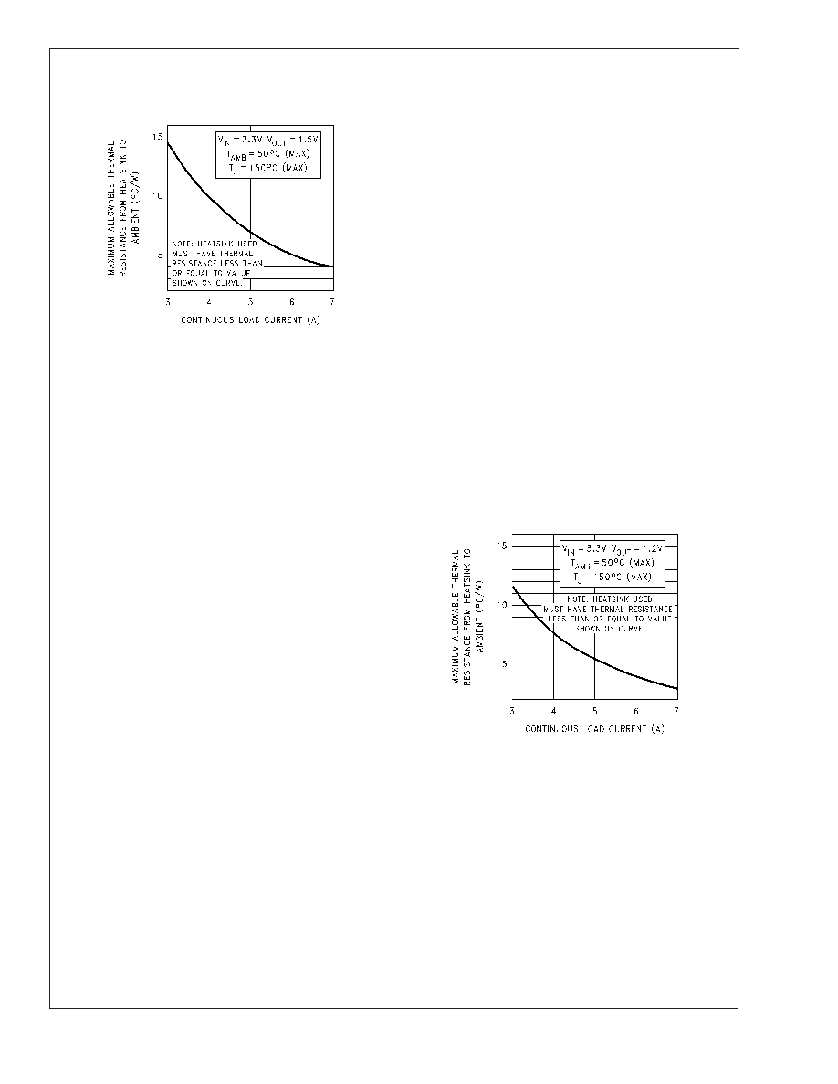
HEATSINKING
The 1.2V design needs a little more heatsinking because the
lower output voltage means more power dissipation in Q4 at
any value of load current.
Figure 7 shows the maximum allowable values of thermal
resistance (from heatsink-to-ambient) that must be provided
for various values of the load current.
Q1 DRIVE CIRCUITRY
In the circuit shown in Figure 1, the output of U1 drives the
base of Q1 with current when the voltage at V
OUT reaches
the regulation point. As Q1 turns ON, it steals drive from Q2
which holds the loop in regulation.
The circuit of Figure 2 uses a different drive configuration for
Q1, required because of the lower voltage across U1.
With only 1.2V across U1, the OUT pin of the LM3460
cannot swing up high enough in voltage to turn on the V
BE of
Q1.
01260312
FIGURE 6. Q4 Heatsink Requirements for Circuit
Shown in Figure 1
01260313
FIGURE 7. Q4 Heatsink Requirements for Circuit
shown in Figure 2
LM3460
www.national.com
7
相关PDF资料 |
PDF描述 |
|---|---|
| LM4040B25IDBZR | 1-OUTPUT TWO TERM VOLTAGE REFERENCE, 2.5 V, PDSO3 |
| LM4040C41ILP | 1-OUTPUT TWO TERM VOLTAGE REFERENCE, 4.096 V, PBCY3 |
| LM4040D25QDBZR | 1-OUTPUT TWO TERM VOLTAGE REFERENCE, 2.5 V, PDSO3 |
| LM4040D30ILPR | 1-OUTPUT TWO TERM VOLTAGE REFERENCE, 3 V, PBCY3 |
| LM4040B10IDBZTG4 | 1-OUTPUT TWO TERM VOLTAGE REFERENCE, 10 V, PDSO3 |
相关代理商/技术参数 |
参数描述 |
|---|---|
| LM3460M5X-1.2 | 功能描述:IC CONTROLLER PRECISION SOT23-5 RoHS:是 类别:集成电路 (IC) >> 接口 - 控制器 系列:- 标准包装:4,900 系列:- 控制器类型:USB 2.0 控制器 接口:串行 电源电压:3 V ~ 3.6 V 电流 - 电源:135mA 工作温度:0°C ~ 70°C 安装类型:表面贴装 封装/外壳:36-VFQFN 裸露焊盘 供应商设备封装:36-QFN(6x6) 包装:* 其它名称:Q6396337A |
| LM3460M5X-1.5 | 功能描述:IC CONTROLLER PRECISION SOT23-5 RoHS:是 类别:集成电路 (IC) >> 接口 - 控制器 系列:- 标准包装:4,900 系列:- 控制器类型:USB 2.0 控制器 接口:串行 电源电压:3 V ~ 3.6 V 电流 - 电源:135mA 工作温度:0°C ~ 70°C 安装类型:表面贴装 封装/外壳:36-VFQFN 裸露焊盘 供应商设备封装:36-QFN(6x6) 包装:* 其它名称:Q6396337A |
| LM3460M5X15 | 制造商:Texas Instruments 功能描述:* |
| LM3463 | 制造商:TI 制造商全称:Texas Instruments 功能描述:Dynamic Headroom Controller with Thermal Control Interface and Individual Channel Dimming Control |
| LM3463_12 | 制造商:TI 制造商全称:Texas Instruments 功能描述:LM3463 Dynamic Headroom Controller with Thermal Control Interface and Individual Channel Dimming Control |
发布紧急采购,3分钟左右您将得到回复。