- 您现在的位置:买卖IC网 > PDF目录79679 > LM3460M5X-1.2/NOPB (NATIONAL SEMICONDUCTOR CORP) 1-OUTPUT THREE TERM VOLTAGE REFERENCE, 1.22 V, PDSO5 PDF资料下载
参数资料
| 型号: | LM3460M5X-1.2/NOPB |
| 厂商: | NATIONAL SEMICONDUCTOR CORP |
| 元件分类: | 基准电压源/电流源 |
| 英文描述: | 1-OUTPUT THREE TERM VOLTAGE REFERENCE, 1.22 V, PDSO5 |
| 封装: | SOT-23, 5 PIN |
| 文件页数: | 4/9页 |
| 文件大小: | 582K |
| 代理商: | LM3460M5X-1.2/NOPB |
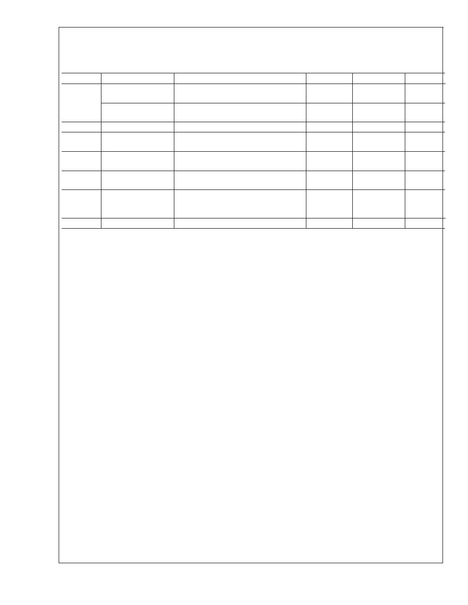
Electrical Characteristics
LM3460-1.2
Specifications with standard type face are for T
J = 25C, and those with boldface type apply over full Operating Tempera-
ture Range. Unless otherwise specified, (+)IN = V
REG,VOUT = 200 mV
Symbol
Parameter
Conditions
Typ (Note 4)
Limit (Note 5)
Units
V
REG
Regulated Voltage
I
OUT = 1 mA
1.220
1.232/ 1.244
1.208/1.196
V (max)
V (min)
Regulated Voltage
Tolerance
I
OUT =1mA
±1/ ±2
% (max)
I
q
Quiescent Current
I
OUT = 1 mA
85
125/150
A (max)
G
m
Transconductance
I
OUT /
V
REG
20A
≤ I
OUT
≤ 1mA
V
OUT = 200 mV
3.3
1/0.5
mA/mV
(min)
V
SAT
Output Saturation
V
IN =VREG + 100 mV
I
OUT =1mA
0.8
0.95
V (max)
I
L
Output Leakage
Current
V
IN =VREG 100 mV
V
OUT =0V
0.1
0.5/1.0
A (max)
R
F
Internal Feedback
Resistor (See
Functional Diagram)
10
12.5
7.5
k
(max)
k
(min)
E
n
Output Noise Voltage
I
OUT = 1 mA, 10 Hz
≤ f ≤ 10kHz
50
V (rms)
Note 1: Absolute Maximum Ratings are limits beyond which damage to the device may occur. Operating Ratings indicate conditions for which the device is intended
to be functional, but do not guarantee specific performance limits. For guaranteed specifications and test conditions, see the Electrical Characteristics. The
guaranteed specifications apply only for the test conditions listed. Some performance characteristics may degrade when the device is not operated under the listed
test conditions.
Note 2: The maximum power dissipation must be derated at elevated temperatures and is dictated by TJmax (maximum junction temperature), θJA (junction ot
ambient thermal resistance), and TA (ambient temperature). The maximum allowable power dissipation at any temperature is (PDmax =(TJmax TA)/θJA)orthe
number given in the Absolute Maximum Ratings, whichever is lower. The typical thermal resistance
θJA when soldered to a printed circuit board is approximately 330
C/W.
Note 3: The human body model is a 100 pF capacitor discharged through a 1.5 k
resistor into each pin.
Note 4: Typical numbers are at 25C and represent the most likely parametric norm.
Note 5: Limits are 100% production tested at 25C. Limits over the operating temperature range are guaranteed through correlation using Statistical Quality Control
(SQC) methods. The limits are used to calculate National’s Average Outgoing Quality Level (AOQL).
Note 6: VSAT =VREG VOUT, when the voltage at the IN pin is forced 100mV above the nominal regulating voltage (VREG).
LM3460
www.national.com
4
相关PDF资料 |
PDF描述 |
|---|---|
| LM385M3-1.2X | 1-OUTPUT TWO TERM VOLTAGE REFERENCE, 1.235 V, PDSO3 |
| LT1680SW | SWITCHING CONTROLLER, 200 kHz SWITCHING FREQ-MAX, PDSO16 |
| LES008ZD18N | 1-OUTPUT 15 W DC-DC REG PWR SUPPLY MODULE |
| LES008ZD19N | 1-OUTPUT 15 W DC-DC REG PWR SUPPLY MODULE |
| LM4050BIX3-3.0+T | 1-OUTPUT TWO TERM VOLTAGE REFERENCE, 3 V, PDSO3 |
相关代理商/技术参数 |
参数描述 |
|---|---|
| LM3460M5X15 | 制造商:Texas Instruments 功能描述:* |
| LM3463 | 制造商:TI 制造商全称:Texas Instruments 功能描述:Dynamic Headroom Controller with Thermal Control Interface and Individual Channel Dimming Control |
| LM3463_12 | 制造商:TI 制造商全称:Texas Instruments 功能描述:LM3463 Dynamic Headroom Controller with Thermal Control Interface and Individual Channel Dimming Control |
| LM3463EVM | 功能描述:LED 照明开发工具 LM3463EVM Eval Mod RoHS:否 制造商:Fairchild Semiconductor 产品:Evaluation Kits 用于:FL7732 核心: 电源电压:120V 系列: 封装: |
| LM3463EVM | 制造商:Texas Instruments 功能描述:EVAL BOARD, LM3463 200mA LED DRIVER |
发布紧急采购,3分钟左右您将得到回复。