- 您现在的位置:买卖IC网 > PDF目录98001 > LM3524DMWC (NATIONAL SEMICONDUCTOR CORP) 0.2 A SWITCHING CONTROLLER, 350 kHz SWITCHING FREQ-MAX, UUC PDF资料下载
参数资料
| 型号: | LM3524DMWC |
| 厂商: | NATIONAL SEMICONDUCTOR CORP |
| 元件分类: | 稳压器 |
| 英文描述: | 0.2 A SWITCHING CONTROLLER, 350 kHz SWITCHING FREQ-MAX, UUC |
| 封装: | WAFER |
| 文件页数: | 19/22页 |
| 文件大小: | 728K |
| 代理商: | LM3524DMWC |
Functional Description
INTERNAL VOLTAGE REGULATOR
The LM3524D has an on-chip 5V, 50 mA, short circuit pro-
tected voltage regulator. This voltage regulator provides a
supply for all internal circuitry of the device and can be used
as an external reference.
For input voltages of less than 8V the 5V output should be
shorted to pin 15, V
IN, which disables the 5V regulator. With
these pins shorted the input voltage must be limited to a
maximum of 6V. If input voltages of 6V–8V are to be used, a
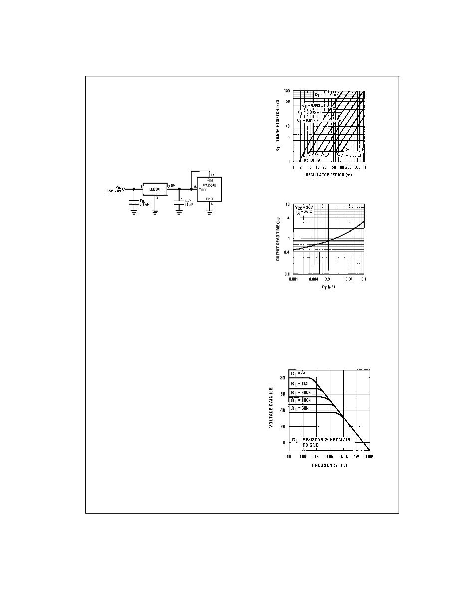
pre-regulator, as shown in
Figure 1, must be added.
OSCILLATOR
The LM3524D provides a stable on-board oscillator. Its fre-
quency is set by an external resistor, R
T and capacitor, CT.A
graph of R
T,CT vs oscillator frequency is shown is Figure 2.
The oscillator’s output provides the signals for triggering an
internal flip-flop, which directs the PWM information to the
outputs, and a blanking pulse to turn off both outputs during
transitions to ensure that cross conduction does not occur.
The width of the blanking pulse, or dead time, is controlled
by the value of C
T, as shown in Figure 3. The recommended
values of R
T are 1.8 k to 100 k, and for CT, 0.001 F to
0.1 F.
If two or more LM3524D’s must be synchronized together,
the easiest method is to interconnect all pin 3 terminals, tie
all pin 7’s (together) to a single C
T, and leave all pin 6’s open
except one which is connected to a single R
T. This method
works well unless the LM3524D’s are more than 6" apart.
A second synchronization method is appropriate for any cir-
cuit layout. One LM3524D, designated as master, must have
its R
TCT
set for the correct period. The other slave
LM3524D(s) should each have an R
TCT set for a 10% longer
period. All pin 3’s must then be interconnected to allow the
master to properly reset the slave units.
The oscillator may be synchronized to an external clock
source by setting the internal free-running oscillator fre-
quency 10% slower than the external clock and driving pin 3
with a pulse train (approx. 3V) from the clock. Pulse width
should be greater than 50 ns to insure full synchronization.
ERROR AMPLIFIER
The error amplifier is a differential input, transconductance
amplifier. Its gain, nominally 86 dB, is set by either feedback
or output loading. This output loading can be done with ei-
ther purely resistive or a combination of resistive and reac-
tive components. A graph of the amplifier’s gain vs output
load resistance is shown in
Figure 4.
The output of the amplifier, or input to the pulse width modu-
lator, can be overridden easily as its output impedance is
very high (Z
O 5M). For this reason a DC voltage can be
DS008650-10
*Minimum CO of 10 F required for stability.
FIGURE 1.
DS008650-5
FIGURE 2.
DS008650-6
FIGURE 3.
DS008650-7
FIGURE 4.
www.national.com
6
相关PDF资料 |
PDF描述 |
|---|---|
| LM3621M-3.0X | BATTERY CHARGE CONTROLLER, PDSO16 |
| LM3621MX-3.0 | BATTERY CHARGE CONTROLLER, PDSO16 |
| LM3647M | POWER SUPPLY MANAGEMENT CKT, PDSO8 |
| LM385BDR-1-2E4 | 1-OUTPUT TWO TERM VOLTAGE REFERENCE, 1.235 V, PDSO8 |
| LM385PW-2-5 | 1-OUTPUT TWO TERM VOLTAGE REFERENCE, 2.5 V, PDSO8 |
相关代理商/技术参数 |
参数描述 |
|---|---|
| LM3524DMX | 功能描述:电压模式 PWM 控制器 RoHS:否 制造商:Texas Instruments 输出端数量:1 拓扑结构:Buck 输出电压:34 V 输出电流: 开关频率: 工作电源电压:4.5 V to 5.5 V 电源电流:600 uA 最大工作温度:+ 125 C 最小工作温度:- 40 C 封装 / 箱体:WSON-8 封装:Reel |
| LM3524DMX/NOPB | 功能描述:电压模式 PWM 控制器 RoHS:否 制造商:Texas Instruments 输出端数量:1 拓扑结构:Buck 输出电压:34 V 输出电流: 开关频率: 工作电源电压:4.5 V to 5.5 V 电源电流:600 uA 最大工作温度:+ 125 C 最小工作温度:- 40 C 封装 / 箱体:WSON-8 封装:Reel |
| LM3524DN | 功能描述:电压模式 PWM 控制器 RoHS:否 制造商:Texas Instruments 输出端数量:1 拓扑结构:Buck 输出电压:34 V 输出电流: 开关频率: 工作电源电压:4.5 V to 5.5 V 电源电流:600 uA 最大工作温度:+ 125 C 最小工作温度:- 40 C 封装 / 箱体:WSON-8 封装:Reel |
| LM3524DN | 制造商:Texas Instruments 功能描述:ENHANCED PWM CONTROLLER 3524 DIP |
| LM3524DN/NOPB | 功能描述:电压模式 PWM 控制器 RoHS:否 制造商:Texas Instruments 输出端数量:1 拓扑结构:Buck 输出电压:34 V 输出电流: 开关频率: 工作电源电压:4.5 V to 5.5 V 电源电流:600 uA 最大工作温度:+ 125 C 最小工作温度:- 40 C 封装 / 箱体:WSON-8 封装:Reel |
发布紧急采购,3分钟左右您将得到回复。