- 您现在的位置:买卖IC网 > PDF目录80197 > LM3544M-H/NOPB (NATIONAL SEMICONDUCTOR CORP) 2-CHANNEL POWER SUPPLY SUPPORT CKT, PDSO16 PDF资料下载
参数资料
| 型号: | LM3544M-H/NOPB |
| 厂商: | NATIONAL SEMICONDUCTOR CORP |
| 元件分类: | 电源管理 |
| 英文描述: | 2-CHANNEL POWER SUPPLY SUPPORT CKT, PDSO16 |
| 封装: | LEAD FREE, SOIC-16 |
| 文件页数: | 2/13页 |
| 文件大小: | 785K |
| 代理商: | LM3544M-H/NOPB |
Application Information (Continued)
tantalum capacitor is recommended. The input supply
should be further bypassed with a 0.01 F - 0.1 F ceramic
capacitor, placed close to the device. The ceramic capacitor
reduces ringing on the supply that can occur when a short is
present at the output of a port.
EXTENDING THE FAULT FLAG DELAY
While the 7 ms (typical) internal delay in reporting flag con-
ditions is adequate for most applications, the delay can be
extended by connecting external RC filters to the FLAG pins,
as shown in Figure 5.
POWER DISSIPATION AND JUNCTION TEMPERATURE
A few simple calculations will allow a designer to calculate
the approximate operating temperature of the LM3544 for a
given application. The large currents possible through the
low resistance power MOSFET combined with the high ther-
mal resistance of the SOIC package, in relation to power
packages, make this estimate an important design step.
Begin the estimate by determining R
ON at the expected
operating temperature using the graphs in the Typical Per-
formance Characteristics section of this datasheet. Next,
calculate the power dissipation through the switch with
PD=R
ON *IDS
2
(1)
Note: Equation for power dissipation neglects portion that
comes from LM3544 quiescent current because this value
will almost always be insignificant.
Using this figure, determine the junction temperature with
T
J =PD*
θ
JA +TA.
(2)
Where:
θ
JA = SOIC Thermal Resistance: 130C/W and TA = Ambient
Temperature (C).
Compare the calculated temperature with the expected tem-
perature used to estimate R
ON. If they do not reasonably
match, re-estimate R
ON using a more appropriate operating
temperature and repeat the calculations. Reiterate as nec-
essary.
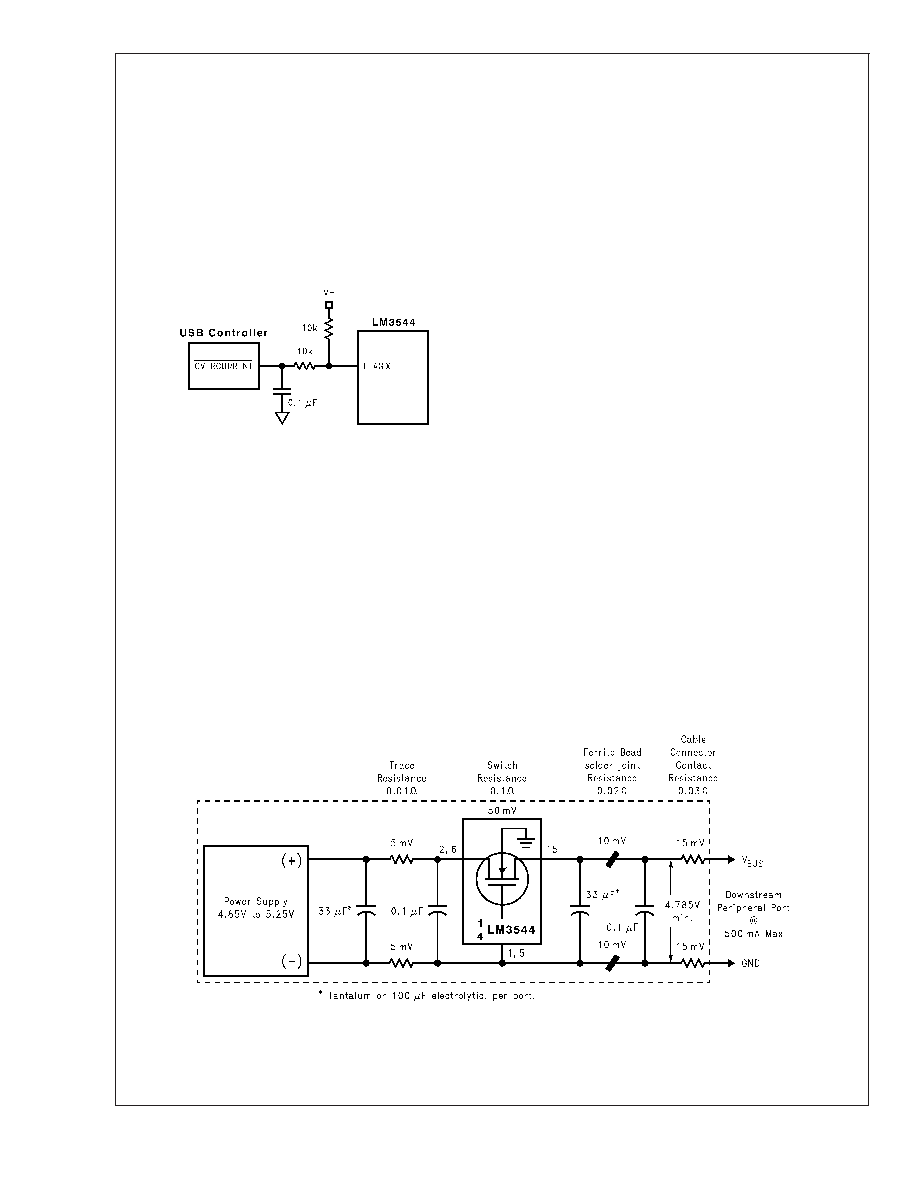
PCB LAYOUT CONSIDERATIONS
In order to meet the USB requirements for voltage drop,
droop and EMI, each component used in this circuit must be
evaluated for its contribution to the circuit performance.
These principles are illustrated in Figure 6. The following
PCB layout rules and guidelines are recommended
1.
Place the switch as close to the USB connector as
possible. Keep all V
bus traces as short as possible and
use at least 50-mil, 1 ounce copper for all V
bus traces.
Solder plating the traces will reduce the trace resistance.
2.
Avoid vias as much as possible. If vias are used, use
multiple vias in parallel and/or make them as large as
possible.
3.
Place the output capacitor and ferrite beads as close to
the USB connector as possible.
4.
If ferrite beads are used, use wires with minimum resis-
tance and large solder pads to minimize connection
resistance.
10120828
FIGURE 5. Typical Circuit for Lengthening the Internal
Flag Delay
10120827
FIGURE 6. Self-Powered Hub Connections and Per-Port Voltage Drop
LM3544
www.national.com
10
相关PDF资料 |
PDF描述 |
|---|---|
| LMD12D | 2-OUTPUT 75 W DC-DC REG PWR SUPPLY MODULE |
| LMD100S | 1-OUTPUT 75 W DC-DC REG PWR SUPPLY MODULE |
| LK1001-7D3T | 1-OUTPUT 150 W AC-DC REG PWR SUPPLY MODULE |
| LK1001-7ED6B1 | 1-OUTPUT 150 W AC-DC REG PWR SUPPLY MODULE |
| LK1001-7EPV0 | 1-OUTPUT 150 W AC-DC REG PWR SUPPLY MODULE |
相关代理商/技术参数 |
参数描述 |
|---|---|
| LM3544M-L | 功能描述:电源开关 IC - USB RoHS:否 制造商:Micrel 电源电压-最小:2.7 V 电源电压-最大:5.5 V 最大工作温度:+ 85 C 最小工作温度:- 40 C 封装 / 箱体:SOIC-8 封装:Tube |
| LM3544M-L/NOPB | 功能描述:电源开关 IC - USB RoHS:否 制造商:Micrel 电源电压-最小:2.7 V 电源电压-最大:5.5 V 最大工作温度:+ 85 C 最小工作温度:- 40 C 封装 / 箱体:SOIC-8 封装:Tube |
| LM3544MX-H | 制造商:NSC 制造商全称:National Semiconductor 功能描述:Quad Port USB Power Distribution Switch and Over-Current Protection |
| LM3544MX-H/NOPB | 功能描述:IC USB QUAD PORT SWITCH 16-SOIC RoHS:是 类别:集成电路 (IC) >> PMIC - 电源分配开关 系列:- 特色产品:XRP252 Switches 标准包装:1 系列:- 类型:高端开关 输出数:2 Rds(开):140 毫欧 内部开关:是 电流限制:1.15A 输入电压:1.75 V ~ 5.5 V 工作温度:-40°C ~ 85°C 安装类型:表面贴装 封装/外壳:10-WFDFN 裸露焊盘 供应商设备封装:10-TDFN(3x3) 包装:Digi-Reel® 其它名称:1016-1691-6 |
| LM3544MX-L | 功能描述:电源开关 IC - USB RoHS:否 制造商:Micrel 电源电压-最小:2.7 V 电源电压-最大:5.5 V 最大工作温度:+ 85 C 最小工作温度:- 40 C 封装 / 箱体:SOIC-8 封装:Tube |
发布紧急采购,3分钟左右您将得到回复。