- 您现在的位置:买卖IC网 > PDF目录44553 > LM3647IMX (NATIONAL SEMICONDUCTOR CORP) 1-CHANNEL POWER SUPPLY SUPPORT CKT, PDSO20 PDF资料下载
参数资料
| 型号: | LM3647IMX |
| 厂商: | NATIONAL SEMICONDUCTOR CORP |
| 元件分类: | 电源管理 |
| 英文描述: | 1-CHANNEL POWER SUPPLY SUPPORT CKT, PDSO20 |
| 封装: | PLASTIC, SOIC-20 |
| 文件页数: | 11/14页 |
| 文件大小: | 271K |
| 代理商: | LM3647IMX |
4.0 Functional Description (Continued)
tied to V
CC (PWM “fast” frequency) or a constant current
source when tied to GND (PWM “slow” frequency). When
configured for Li-Ion batteries, SEL3 switches between 4.1V
cells or 4.2V cells.
Note: SEL3 must be hard wired to VCC if a charger that supports both Li-Ion
and Ni-Cd/Ni-MH is implemented.
SEL3
PWM Output Frequency Select
output SEL2 = V
CC (NiMH) or GND (NiCd)
V
CC
Current feedback (“fast” PWM frequency)
GND
No current feedback (external constant
current source) (“slow” PWM frequency)
SEL3
Li-Ion Cell Voltage Select
output SEL2 = Open (Li-Ion)
V
CC
4.2V/cell
GND
4.1V/cell
Note: Current feedback is automatically selected, if LM3647 is configured for
Li-Ion charging (pin SEL2 open).
SEL4 is connected to a RC-network that determines the
charge time-outs. This RC-network is also connected to the
output LED1. (See Section 4.3.2 for details).
RCIN is a high-speed timing pin connected to a RC-network,
used to drive the charger at the right operating frequency.
GND is the ground pin.
V
CC is the power-supply pin. This pin should have a 100 nF
decoupling capacitor tied to GND.
RESET is a reset pin.
LED1 is an active-low output used to indicate charge phase.
It is also used when measuring the charge timeout value.
LED2 is an active-low output used to indicate charge or
discharge. It also sends out digitally what the LM3647 has
read at the mode selection pins and charge timeout.
LED3 is an active-low output used to indicate charge start/
stop and error.
V
REF is the voltage reference analog input. The LM3647
uses this pin as a reference when measuring the other
analog inputs. V
REF has to be connected to a 2.5V voltage
reference (e.g., LM4040A - 2.5).
CEXT is a timing pin used by the LM3647, it must be
connected to a low loss capacitor (polyester).
CEL is an analog input that measures the battery voltage via
a resistor divider network.
CS is an analog input that is connected to a differential
amplifier that measures the voltage over a small current
sensing resistor, when used in conjunction with current feed-
back power supply. When the LM3647 is used with a con-
stant current power supply, CS should be connected to the
2.5V voltage reference (pin V
REF).
TEMP is an analog input that is connected to the tempera-
ture sensing NTC-resistor (is used). If no temperature sen-
sor is used, the input must be connected to a voltage be-
tween 0.5V to 2.2V.
DISCHG is a digital output that controls a power-FET that
discharges the batteries before charging them. If the dis-
charge function is not used, leave this pin unconnected.
SYSOK is an open drain output that resets the LM3647 in
the rare case of an internal illegal operating condition. This
pin is connected to the RESET pin to increase reliable
operation of the device in hostile operating environments
(e.g., noisy environments).
BUZZER is a digital output that controls a small FET and
turns an optional buzzer on and off. The buzzer must have
it’s own oscillator drive circuitry.
PWM is a digital output that controls the charge voltage or
turns the external current source on and off (depending on
mode-selection).
4.3 CONFIGURATIONS
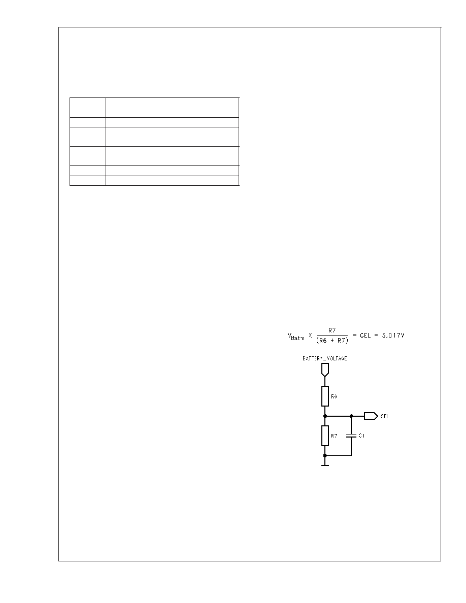
4.3.1 Maximum Battery Voltage
The maximum battery voltage corresponds to the number of
battery cells. The resistor network in the figure below scales
the battery voltage to a level suitable for the LM3647. For
Ni-Cd/Ni-MH batteries the tolerance of the network is not
critical, and only defines the maximum battery voltage
(which is used as a backup termination method). For Li-Ion
batteries the network must be more accurate, and resistors
with low tolerances must be used (1% or better).
Ni-Cd/Ni-MH
Each battery cell is at nominal voltage 1.2V, but the critical
voltage is rather the maximum voltage per cell specified at
1.85V. The maximum cell voltage is used for maximum
voltage error termination. If a Ni-Cd/Ni-MH cell fails, it either
becomes shorted or goes high impedance. In the case of
high impedance the cell voltage will reach 1.85V. By multi-
plying the number of cells with the maximum cell voltage, the
Maximum Battery Voltage (V
Batm) is achieved.
When the maximum battery voltage has been determined,
the voltage divider network can be dimensioned using the
following formula (SEL2 connected to V
CC or GND):
10131807
LM3647
www.national.com
6
相关PDF资料 |
PDF描述 |
|---|---|
| LM3655TLX | 1-CHANNEL POWER SUPPLY SUPPORT CKT, BGA25 |
| LM3661TLX-1.40 | 0.65 A SWITCHING REGULATOR, 675 kHz SWITCHING FREQ-MAX, PBGA10 |
| LM3661TL-1.25 | 0.454 A SWITCHING REGULATOR, 675 kHz SWITCHING FREQ-MAX, PBGA10 |
| LM3668SD-3.3/NOPB | 2.05 A DUAL SWITCHING CONTROLLER, 2500 kHz SWITCHING FREQ-MAX, DSO12 |
| LM368N-5.0 | 1-OUTPUT TWO TERM VOLTAGE REFERENCE, 5 V, PDIP8 |
相关代理商/技术参数 |
参数描述 |
|---|---|
| LM3647M | 制造商:未知厂家 制造商全称:未知厂家 功能描述:Battery Management |
| LM3648EVM | 功能描述:LM3648 1, Non-Isolated Output LED Driver Evaluation Board 制造商:texas instruments 系列:- 零件状态:有效 电流 - 输出/通道:1.5A 输出和类型:1,非隔离 电压 - 输出:- 特性:I2C 电压 - 输入:2.5 V ~ 5.5 V 所含物品:板 使用的 IC/零件:LM3648 标准包装:1 |
| LM3648TTYFFR | 功能描述:LED 驱动器 IC 1 输出 DC DC 稳压器 升压(升压) 调光 1.5A(闪存) 12-DSBGA 制造商:texas instruments 系列:- 包装:剪切带(CT) 零件状态:在售 类型:DC DC 稳压器 拓扑:升压(升压) 内部开关:是 输出数:1 电压 - 供电(最低):2.5V 电压 -?供电(最高):5.5V 电压 - 输出:- 电流 - 输出/通道:1.5A(闪存) 频率:4MHz 调光:- 应用:照相机闪光灯 工作温度:-40°C ~ 85°C(TA) 安装类型:表面贴装 封装/外壳:12-UFBGA,DSBGA 供应商器件封装:12-DSBGA 标准包装:1 |
| LM3648YFFR | 功能描述:LED 驱动器 IC 1 输出 DC DC 稳压器 升压(升压) 1.5A(闪存) 12-DSBGA 制造商:texas instruments 系列:- 包装:剪切带(CT) 零件状态:有效 类型:DC DC 稳压器 拓扑:升压(升压) 内部开关:是 输出数:1 电压 - 供电(最低):2.5V 电压 -?供电(最高):5.5V 电压 - 输出:- 电流 - 输出/通道:1.5A(闪存) 频率:4MHz 调光:- 应用:照相机闪光灯 工作温度:-40°C ~ 85°C(TA) 安装类型:表面贴装 封装/外壳:12-UFBGA,DSBGA 供应商器件封装:12-DSBGA 标准包装:1 |
| LM3649MHE-AA/NOPB | 制造商:Texas Instruments 功能描述: |
发布紧急采购,3分钟左右您将得到回复。